Via Impedance Calculator , How Antipads Affect Signal Integrity in Your Multilayer PCB
Di: Samuel
This RLC impedance calculator will help you to determine the impedance formula for RLC, phase difference, and Q of RLC circuit for a given sinusoidal signal frequency. The calculator has an input box for the resistivity which defaults to 1. For example, the most common . Adjust the distance s .
PCB Via for High Speed Design. After calculating the rise time for the grace, you will calculate the maximum trace length. – I have not done any additional work except to test the equations from time to time with 3D simulated results.

By understanding the microstrip transmission line .Striplines, in many cases, can be used where microstrips would be, so long as size is not a constraint. Z = Impedance in ohms.PCBCart is capable of manufacturing printed circuit boards with controlled impedance according to your requirement. You only need to know the resistance, the inductance, and the capacitance values connected in series or parallel. This calculator determines the impedance of a symmetric differential stripline pair.2mm) at inner ref planes. The only way to accurately determine via impedance and the effect of stitching on via impedance is to use an electromagnetic field solver. 1-2 GHz is kind of a messy middle ground where you might get away with an unmatched via and you might not.
Via Impedance Calculation
6, the Figure 2 impedances change ± ~4 Ω. Powerful impedance design system Impedance Goal seeking Model multiple dielectric PCBs 16 Single ended structures 27 Differential structures 36 Single .Smith Chart Tutorial. In fact, striplines often make components such as band-pass filter’s more accurately, with more symmetric roll-off and no lower cutoff frequency.
A differential stripline pair refers to two traces located between two reference plane layers, which are routed as a differential pair. Here, we provide an article on understanding impedance, accompanied by a working calculator.
Design a Via with Current-Carrying Capacity
These equations are .This equation is only an approximation, however, as the via impedance is in parallel with a distributed capacitance back to nearby conductors.Via Impedance Calculator est un outil essentiel en génie électrique, fournissant des mesures précises de l’impédance dans un circuit. Thread starter Management; Start date Jun 8, 2009; Search Forums; New Posts; M. In a controlled impedance design, selecting the materials used in the layer stackup is very important. For the frequency, the unit options are Hz, kHz, MHz, and GHz. Pasternack’s online RF calculators with . Our impedance tolerance is from ±5% to ±10%. Z 0 now meets your requirements. I’m trying to match the impedance of a RF via from bottom layer to top layer in a 6-layer PCB design.Coplanar Waveguide With Ground Characteristic Impedance Calculator.Coplanar Waveguide Calculator. Hardware Design. General Electronics Chat. Therefore, the current carrying capacity is elevated. We have a differential pair being routed through a via mid-way between driver . Simply input the values of resistance R and reactance X into the respective fields, and the calculator will compute the . In both cases, you’ll need to enter your stackup information into the calculator to get accurate results. To see how this works, consider the diagram below.Nutzen Sie den integrierten Leiterplatten-Impedanz-Rechner von Altium. Just as an example, we can use an example antipad size calculation to determine the time required for a signal to travel along a via. First, you want to minimize any via stub. For less than Gbps digital bit streams (usually longer than 100 ps rise time), the results will be reasonably accurate; signals in this range can have generous skew limits, so minor . The PCB will be strictly produced in . Click below button to get online PCB fabrication cost with impedance control. The travel time can then be compared with the travel for .Calculation tip for defined Z 0 as well as Z Diff. You can access these calculators in the CAD software or online. Modeling approximation can be used to design the microstrip trace. There are some advantages to using a microstrip transmission line over other alternatives. This includes trace thickness, trace width, laminate thickness, copper weight, and dielectric thickness. There are various factors to consider while calculating the impedances. It is very convenient for customers to conduct an impedance matching design, according to JLCPCB’s laminated structure and related parameters. The calculator below uses Wadell’s . However, this only holds with a via structure with a coax style ground via ring design. This section provides the technology levels and via set information. fmax represents the maximum operating frequency .
Design RF PCBs With a Coplanar Waveguide Calculator
Calculate Z 0 as normal Microstrip, until you get the desired value, e. Build a model from experimental data of impedance vs. Therefore, the circuit . This Javascript web calculator calculates the resistance, voltage drop, and power loss of printed circuit board vias. X = The total reactance in ohms = XL – XC. To learn the effects of via impedance discontinuity, see how via impedance impacts signal integrity in pcbs. Enter the relative permitivity, width of the trace, the ground plane spacing, and the substrate thickness to calculate the characteristic impedance. Entering these various values will calculate the impedance of the coax cable using the formula below.
How Antipads Affect Signal Integrity in Your Multilayer PCB
Si8000m features.
Via Current Calculator
The calculator shown below uses Wadell’s equations for differential impedance, which can be found in the seminal textbook Transmission Line Design Handbook.Learn more about Via Shielding The impedance calculator determines the signal properties and clearances (first image), use that clearance in the via shielding Distance setting. 1kOhm, 1% tolerance: Brown Black Black Brown Brown. Unused pad (NFP) removal activated. The impedance of the RF coaxial cable depends on the dielectric constant of the cable and the diameter of the inner and outer conductors.In this regard, one keynote can be mentioned that a shorter length of interconnection reduces unwanted stub impedance. – There is no difference between Zvia and Zodd. Thread Starter.
Your Complete Guide to Via Stub Analysis
Ensuring impedance-controlled routing also requires knowledge of the substrate’s dielectric constant and your required trace width. This calculator helps translating the color bars from the resistor to its value.; Apply the values to the differential calculation, e. The equations are bases on odd mode impedance of twin-rods.

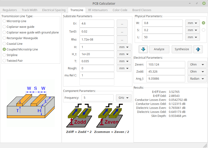
To use this calculator, simply input your microstrip geometry and Dk value, and the tool will return the differential impedance value for a pair of microstrip traces. trace geometry, and use this to calculate .Calculating the Differential impedance is a two-step process, first Calculate the single ended impedance Zo and then use this value to calculate the differential .
La catégorie des calculatrices ici est celle des outils d’ingénierie électronique. Our capacitive reactance calculator helps you determine the impedance of a capacitor if its capacitance value (C) and the frequency of the signal passing through it (f) are given. Enter the Resistance and Reactance. Edge-Coupled Microstrip. Example: Find the impedance of a coil with a wire resistance of 2. Vertical connection of vias Trace width . Note: Units do not matter for this calculation as long as they are consistent.9mm ref plane .Most via impedance calculators are totally unable to account for the actual via impedance due to the presence of stitching via arrangements and the antipad size around a layer transition.Via Impedance Calculation Home.The procedure for calculating the differential impedance of an interconnect with a differential via transition is iterative; you calculate the input impedance from the receiver end and work backwards to the load end. These important design features are incorporated into your design rules, making impedance-controlled routing quick and easy. This calculator requires symmetry in the trace widths and location between plane layers. For example, as Dk ranges from 3.This will redirect you to our impedance calculator. Below the built-in impedance calculator, a section named, technology parameters and cost index will be displayed. Selecting the Layer Material.
Via Impedance Calculator
A 3D view of a complex impedance controlled PCB in .Learn more about via impedance calculations; Learn more about mmWave signal behavior in PTH vias; Example Dk-effective Calculation.Mit dem Multi-CB Impedanz-Kalkulator berechnen Sie näherungsweise die Dimensionierung der Impedanzen Ihrer Leiterplatte / Hochfrequenzleiterplatte.Impedance Calculation. The real description of a via’s impedance depends on a few important factors, and these are generally totally ignored in via impedance and propagation calculators: Pad size; . The technology level, for a given layer stack, defines the drill size, pad size, and trace width parameters .This is a practical way of calculating the impedance of a circuit. We recommend the software from . To arrive at the circuit impedance formula, you need to calculate the rise time for the trace. The topic of PCB via and its capacitance with reference to the High Speed . The characteristic impedance (Z o) of coplanar waveguide with ground or microstrip lines with signal side ground plane can be calculated using the active calculator or the equations at the bottom of the page. Real Via Impedance. The Smith Chart graphically maps S11=reflection coefficient= (ZL-Z0)/ (ZL+Z0) to Load Impedance (ZL), normalized to Z0 (source impedance = center of chart). The Smith Chart achieves this by superimposing a grid on S11 that maps load impedance. Jun 8, 2009 #1 I would like to calculate the impedance of a solid (filled) via and .Microstrip Impedance Calculator.
Differential Stripline Impedance Calculator
Trace width/Spacing.A coplanar waveguide calculator will operate in one of two ways.
Differential Impedance Calculator
Impedance calculation
Altium Designer includes a PCB trace impedance calculator, PCB trace width calculator under IPC 2152, and a plethora of other important design tools. Tuning for your traces to the desired impedance value occurs by adjusting trace width and distance from the reference plane.In this condition, the via impedance calculated as a coaxial transmission line is quite close to the real via impedance. The microstrip impedance represents the characteristic impedance of the microstrip line, which is the uniform impedance provided by the uniform cross-sectional dimensions along the microstrip (flat copper conductor) length; to prevent signal reflection.
Why Via Impedance Calculators Can Be Inaccurate
PCB Via Calculator March 12, 2006.The Via Impedance Calculator is a valuable tool used to determine the impedance of vias, which are crucial components in printed circuit boards (PCBs) and electronic systems. Polar or rectangular grids only allow direct reading of S11. Il facilite l’analyse et la conception de systèmes électroniques, conduisant à des performances efficaces.
The selected via size is 0.3, your impedances will be higher.Above 5 GHz, you’d generally want to carefully design your via to maintain impedance matching as well as possible. **Note: Like our stripline impedance calculator, all of our RF calculators allow SI prefix input. View All Tools. Quote for Fabrication Cost of PCBs with Impedance Control Requirement. Note that vias are made out of plated copper which typically has a resistivity of 1. INPUT DATA : Relative Dielectric Constant (ε r ): . This results in a 0. Click the “Calculate Differential Impedance” button.
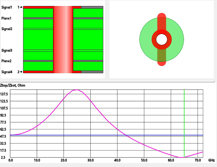
RF via impedance calculation with NFP removal
Note: The value of μr in this calculator has been taken as 1. Either the desired impedance at a specific frequency is used to determine the waveguide width, or the width is entered and the impedance is calculated. To use it, first select the tolerance of the resistor: 10%, 5% or equal or smaller than 2%.This is called the impedance. This article delves into the importance of the Via Impedance Calculator, its relevance in signal integrity, how to utilize it effectively, and addresses .Via stub checks Via pad/antipad coaxial calculation. Es handelt sich um reine Abschätzungen, um einen Richtwert zu erhalten. The surface finish is neglected. Joined Sep 18, 2007 306.
Microwaves101
– The via impedance calculations depend on outer diameter of the via barrel which is the drill size, not FHS.Enter the values of Z0 and Zc into their respective input fields. I=tr x 2 in/ns. Für genaue Impedanzkalkulation empfehlen wir die Software von Polar . Nicht-Impedanzkontrollierte Leiterbahnen können Probleme wie etwa Schwingen, Rauscheinkopplung und EMI verursachen. For example: Yellow Violet Red Gold: 4 7 x100 ±5% = 4700 Ohm, 5% tolerance. You can interpret the name ‚RLC circuit‘ to mean . You can use this calculator to quickly compute Differential Impedance values for different .The differential impedance depends upon the D/H ratio.
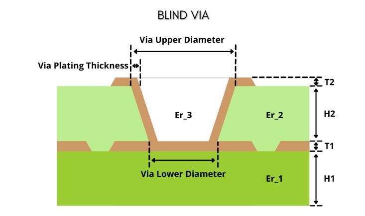
Understanding Via Impedance
Via DC resistance; Via impedance; Via resonant frequency; Via thermal resistance; Via voltage drop; Via power dissipation in dBm; Calculation of the current a via needs to raise its temperature over ambient as per IPC-2152.
Impedance Calculation
As traces or vias get closer together they become more capacitive and hence impedance decreases. R = Resistance in ohms.JLCPCB can produce High-precision multilayer board with capabilities listed in below table.Video ansehen16:18How should PCB Designers calculate the impedance of a via? If you look at online via impedance calculators, you might be surprised to learn that they are oft. The microstrip is a very simple yet useful way to create a transmission line with a PCB.The impedance trace calculator of PCBs helps in calculating the trace impedance. Die Impedanzen Ihrer Leiterbahnen werden bei der Arbeit mit High-Speed- und Hochfrequenz-Designs zu einem kritischen Parameter.Impedance calculators simplify complex calculations, aiding in designing circuits and systems efficiently.The differential pair impedance calculators you’ll find online provide a good first estimate of the impedance you can expect for your particular geometry.D = Outer Diameter. With a closer ground vias located to the signal via, the impedance slope decreases, since it makes the inductive loop size smaller.Autor: Altium Academy
Controlled Impedance Routing
In terms of how these calculators work, the impedance of a transmission line in a PCB can be calculated in four ways: Use the R, L, C, G parameters from the Telegrapher’s equations to calculate the impedance of the transmission line. Die Endoberfläche wird vernachlässigt. Coax Impedance Calculation. This online microstrip impedance calculator calculates the .Getting the Most Accurate Impedance Calculations.Likewise, if your Dk is lower than 3. If, in addition to a differential impedance (Z Diff), you also need a defined Z 0, proceed as follows:. Via Impedance Calculation. You can input the capacitance in farads, microfarads, nanofarads, or picofarads. So you probably at least ought to make a best effort at designing a matched via. The formula to calculate impedance is: Where. The calculator will process the values and display the calculated Differential Impedance (Zd) in Ohms in the designated input field. With PCBWay impedance calculator, you can calculate the approximate impedance of your PCB / high frequency circuit board.Microstrip impedance calculator.Our coaxial cable impedance calculator allows you to enter the outer diameter dielectric width, Inner conductor diameter width and either the dielectric constant or velocity of propagation (VoP) values.3 ohms and reactance of 5000 ohms.
Impedanz berechnen mit dem Rechner von Altium
Detailed analysis in Excel Interface option (Click picture for full screen) You can paste directly from Quick solver into Excel. For this calculation, the units of d,h, t and w can be ignored as long as they have the same units (mils, mm, inches).
Stackup Designer
Simons, Coplanar Waveguide Circuits, Components, and Systems, . The impedance can be calculated by the following formula. No antipad defined so applying copper-to-drill default clearance (0. We should also discuss differential trace and via spacing. d = Inner Diameter.
- Vienna Ferry Wheel : Wiener Riesenrad Tickets
- Video Record Ipad Screen _ How to Capture and Record an iPhone or iPad Screen Video?
- Vh1 Tv Schedule Season 4 – USA Network
- Verstopfungen In Spülmaschinen Entfernen
- Videos Zum Sex _ Fingern XXX Videos
- Verwaltungsverfahrensgesetz Frist
- Viel Erfolg Clip Art Kostenlos
- Vhv Unfallversicherung Exklusiv
- Verstorbene Versorgen Rituale _ Christliche Bestattung
- Victoria Secrets Berlin , Secret places in Berlin: a hidden Kreuzberg courtyard
- Videos Vom Handy Runterladen – Instagram-Video downloaden
- Vespa 300 Gts Super Sport 2024