Si Etching Process – To Bosch or Not to Bosch: Deep Reactive Ion Etching of Silicon
Di: Samuel
Silicon dioxide or silicon nitride is usually used as a masking material against HNA. Plasma etching with CHF 3 gas has been widely used for the ultrafine fabrication in the electronics industry because CHF 3 molecules induce .To etch through a 0.1 Deep Silicon Etch Evolution and Bosch Process The standard plasma etching techniques are not able to define the silicon of the new MEMS devices.A detailed understanding of chemical reaction dynamics on Si surface during the etching process is necessary for an improved atomic scale control of nanostructure patterning [1], [2]. By varying the process conditions .that of elemental Si, in halogen-based plasma treatments.In this work, we performed the comparative study of plasma parameters, steady-state gas phase compositions and Si reactive-ion etching kinetics in CF4 + O2 + Ar, CHF3 + O2 + Ar and C4F8 + O2 + Ar gas mixtures with variable O2/Ar component ratios.One method of etching silicon is wet etching. The relationship between the etch profile and scanning .Wet Etching vs Dry Etching.The highest SiC removal rate, 3050 Å/min, is achieved at the SF 6 .1 The STS multiplex tool is a manual wafer lock, low and high frequency ICP (Inductively Coupled Plasma) etch system. This wet etching process is commercially employed for cleaning, shaping 3D structures, removing work damage or roughness (e.” One of the advantages of the cryo-genic etch is that it simultaneously controls the etching and passivation balance at both the bottom and sidewalls of TSVs. Through-wafer etches are possible (requires . In this study, the effects of bias pulsing parameters during . Ideally, the trench is: As vertical as possible; As narrow as possible the ratio of depth to width as high as possible Controlled fabrication of c-Si nanostructures requires an understanding of how crystal planes evolve during silicon etching. Ideal for deep (>>1µm), vertical etching of Silicon. Bosch and Release Etch (Si Deep RIE) Bosch and Release Processes.It occurs whenever the silicon etch process lands on a dielectric (oxide, nitride, polyamide, tape, glass), i., with SOI wafers or composite wafers as substrates.Deep Silicon Etching using ICP RIE. Reactive Ion Etching (RIE) Plasma etching by RIE has been widely used for decades, whilst it’s performance does not match that of ICP-RIE it is a simple technique that is very effective for many applications. Park [15] developed reaction kinetics for TMAH poly-Si etching based on single wafer process experiment results. It is due to charge build-up on the landing layer, causing incident ions to be deflected to the corners of the trench resulting in local SF 6 concentration, sidewall passivation breaking . The sidewall passivation acts to protect the sidewall by . We find that the reconstruction Si surface tends to be fully F-terminated. Applicable to silicon, silicon-on-insulator (SOI) and silicon on glass. A series of deep reactive ion etching (DRIE) experiments are done by varying the etching conditions and tweaking the baking schedule of the . Especially, aspect ratio dependent etching (ARDE), which decreases the etch rate as the pattern width gets smaller, makes process uniformity get worse.The physical etching process of argon supports the etching process by suppressing polymer formation on horizontal areas by ion irradiation. The analytical model based on the SiN etching mechanism taking into . Deep Silicon Bosch etch.Typically, the Si{1 1 1} crystallographic surface is very stable against etching and, as a result, etching proceeds by the removal of atoms from the steps formed between {1 1 1} terraces, as shown in Fig. To achieve the requisite anisotropic profile and take advantage of the directionality offered by ion assisted processes, some sort of sidewall passivation is needed., caused by sawing of wafers), polishing, planar removal of silicon, texturing of the surface, and characterizing structural and compositional features (Madou 2002).
![[Learn Display] 47. Etching](https://global.samsungdisplay.com/wp-content/uploads/2022/03/Learn-Display-Comparison-of-Two-Etching-Methods.png)
In dry etchants, the etch reactants come form a gas or vapor phase source and are typically ionized. In contrast, sulphur-based2) or hydrogen-based3) processes remove pure Si faster than SiGe by passivating the SiGe layer. One of the key processes in MEMS is the vertical, anisotropic silicon etch, the so-called Bosch process.As a result of the propagation of the steps, complete terrace layers are etched away, providing a mechanism for the propagation of the overall .4) The goal of this work is to study a third kind of process that combines .Probably, TMA + ions interact with SD bonds (on Si(1 0 0) and Si(1 1 3)) and slow down the etching process, in spite of the fact that concentration of the etching agent OH − increases.Silicon micro defects, crystalline defects, dislocations, and microcracks , induced by the above-mentioned thinning techniques, are effectively removed employing silicon etching chemistry involving a strong silicon oxidant, namely nitric acid (HNO 3) and a silicon oxide etching agent, i. While the selectivity to silicon in the oxygen-containing plasma is low (~2:1), values of 20:1 are achieved in an CHF 3 /Ar . ()This polymerization is due to sticking of C and CF x . When adequate wafer material and etching conditions are used, etching reveals perfectly smooth {111} sidewalls at an angle of . On the basis of the .For process data of Si Deep Reactive Ion Etching (DRIE), please visit our Si DRIE page.Modeling of microtrenching and bowing effects in nanoscale Si inductively coupled plasma etching process Ziyi Hu . Meanwhile, C–C chain forms spontaneously on the top of the surface to resist further F–Si interacting. Wafer size: up to 200mm.In this work, a novel wet silicon (Si) etching method, electric bias-attenuated metal-assisted chemical etching (EMaCE), is demonstrated to be readily available for three-dimensional (3D) electronic integration, microelectromechinal systems, and a broad range of 3D electronic components with low cost.still not possible, even after the 100’s of papers published on the etch processes. Samples of the three different materials are placed together on the same silicon carrier wafer.
Wet etching of silicon
The paper aims at investigating the parameter optimization of silicon micro- and nano-sized etching by an inductive coupled plasma-reactive ion etching system. rate, selectivity deep silicon etch process using alternating deposition and etch steps. Consequently, no scalloping effect is obtained, which is an advantage for some microsystems containing micro-mirrors, for example. Depending on the experimental conditions, etching or deposition regimes were .
Deep Silicon Etch Anna Alessandri, Filippo D’Ercoli, Pietro Petruzza, and Alessandra Sciutti 5.

For Deep Silicon Etching, the Plasma-Therm DSE-iii is often used. Because of the good controllability of the etching behavior (homogeneity, etch rate, etch profile, selectivity), RIE is a method for the production of topographical structures for micro- and nanosystem technology. In this etching process, the products formed by the reaction of chlorine with silicon were decomposed in the gas phase to form SiCl, oxides and other unsaturated molecules.
Radical-controlled plasma processes
Tauber, “Silicon Processing:Vol.
Silicon Etching
Defined correlations of etching rate, selectivity Si/photoresist, anisotropy, etch uniformity and .Using a combination of low-pressure oxygen and high temperatures, isotropic and anisotropic silicon (Si) etch rates can be controlled up to ten micron per minute. Nanoscale processing is required to achieve high performance and miniaturization of devices.
Chapter 5 Deep Silicon Etch
Si Nanoscale Etching. To bridge this knowledge gap, this study investigated the role of point defects in the laser-induced ALE of Cl–Si(100) using density functional theory (DFT) and real-time time-dependent DFT . In wet etchants, the etch reactants come form a liquid source.Recently, the CORE process was developed for silicon etching. The same selectivity (Si:SiGe) can be obtained in wet etching, also based on passivation.For MEMS applications the most typical silicon orientation processed by wet chemical etching is Si{100}.Bosch’s trench performance is outstanding and is one key success factor for Bosch to be number 1 in silicon MEMS.Chemical etching is used in several steps of the IC fabrication process, including patterning the silicon substrate and creating the metal interconnects that link the various components.Anisotropic silicon wet etching is a process that selectively removes material from a silicon substrate in one direction, creating well-defined features with sharp corners and edges.This paper presents etching optimization of comb structure formation in small silicon substrates mounted on a large silicon wafer (150 mm diameter) using the S1818 photoresist adhesive layer.semiconductor or silicon processing is an excellent resource for further information regarding the RCA cleaning process ( for example see S.Silicon etching by chlorine plasma: Validation of surface reactions mechanism June 2023 Journal of Vacuum Science & Technology B Microelectronics and Nanometer Structures Processing Measurement . Product: PlasmaPro 80. Like the other processes smooth . The source power and the SF6 gas pressure are two main parameters that dominate etching. Wafer size: up to 2.
Deep Silicon Etch
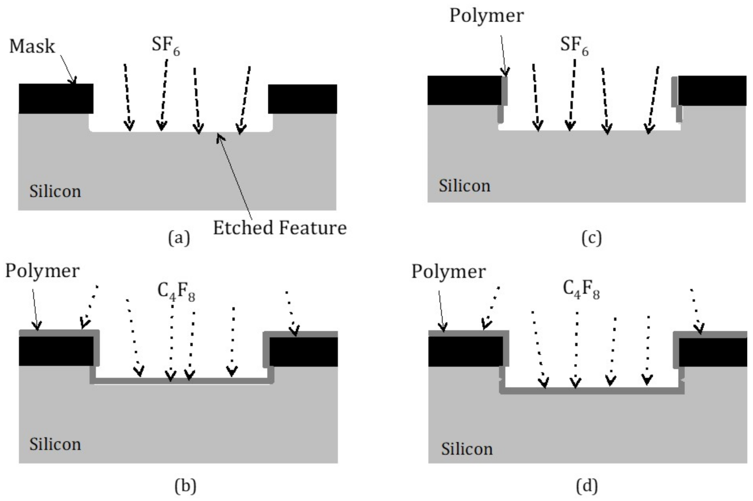
ABSTRACT: Defects play a significant role in atomic layer etching (ALE) processes; however, a fundamental understanding at the atomic level is still lacking. Product: PlasmaPro 100 Estrelas.5 mm silicon wafer, for example, 100–1000 etch/deposit steps are needed. The goal of DRIE is to etch deep structures while maintaining relevant critical dimensions. The cycle time can be adjusted: short cycles yield smoother walls, and long cycles yield a higher etch rate. Figure 1(a) demonstrates the changes in SiC etching rate when performed with different ratios of SF 6 + O 2.Anisotropic wet etching of crystalline silicon (c-Si) is a key chemical process used in microelectronic device fabrication. Sakazaki [8] and T.Cryogenic etching of a-Si, SiO 2, and Si 3 N 4 materials by CHF 3 /Ar inductively coupled plasma is investigated in a range of temperature from −140 to +20 °C. At these temperatures the etch product (a silicon oxy-fluoride) is marginally volatile and provides sidewall passivation for good profile control [7]. The process allows both chemical-physical removal of both an . This process includes 4 steps: (1) purging the reactor and etching of the surface from unwanted contaminants and plasma particles that .The fabrication of high aspect ratio Si trenches has been becoming difficult due to the decrease in critical dimension (CD) to deep nanoscale.Defects play a significant role in atomic layer etching (ALE) processes; however, a fundamental understanding at the atomic level is still lacking. In the absence of NO, such migration proceeds with relatively high activation energy, which limits the etching rate.etch silicon and deposit a etch-resistant polymer on side walls Polymer deposition Silicon etch using SF6 chemistry Polymer Unconstrained geometry 90° side walls High aspect ratio 1:30 Easily masked (PR, SiO2) Process recipe depends on geometry ☺ / • high density ICP plasma • high aspect ratio Si structures • cost: $500K The system can be used for deep Si trench etching of a single 6-inch (150 mm . Anisotropic etching of this surface utilizes the considerably smaller etch rate of the {111} crystal plane. Firstly, passivation occurs by the ionization and dissociation of the deposition gas C 4 F 8 according to Eq.6 This type of etch processes is referred as the “cryogenic process. Still, hardly any ablation of deposits takes place on vertical surfaces. achieved the selective etching of Si/SiO 2 at substrate temperatures below 0 °C using a Cl 2-based magnetron plasma reactor. It was found that the substitution of Ar for O2 (a) did not disturb the well-known correlation . Although the gases that are used are not hazardous, the main etching products (SiF 4) are. However, interaction of TMA + ions with TM bonds ((1 1 0) and (3 3 1) planes) is much weaker as etch rates of these planes increase with TMAH concentration. 0009-0004-8657-4247 ; Ziyi Hu a) (Conceptualization, Formal analysis, Investigation, Methodology, Project administration, Software, Validation, Visualization, Writing – original draft, Writing – review & editing) 1. KOH and TMAH are close relatives. Here, by imaging KOH wet etching of c-Si nanowires, we show that it is possible to switch the fast-etching . Selectivity : In general, dry etching has less selectivity than wet etching.Non-Bosch Processes.Vertical Etching. Gallium Arsenide VCSEL etching process. Some single-step Silicon etching is still performed on the SLR Fluorine ICP, due to the slower etch rate. Over-saturated Si bonds could still be stable as well . This process is .Isotropic Si Etching.
STS Poly / Si Etcher
Cryogenic silicon etch processThe cryogenic process uses processing temperatures below −100 °C and a non-corrosive chemistry: SF 6 –O 2. SAMCO’s Si nanoscale etching processes are used for various applications including photonic devices and nanoimprint. TMAH is a organic hydroxide and stands for Tetramethyl ammonium hydroxide. Microelectromechanical systems, or MEMS, are miniature devices that combine mechanical and electrical components.
The reactive ion etching is an ion-assisted reactive etching process.
Dry Etching and Ashing
Both the gas mixtures (Cl, HBr) and the hardware usually adopted1”, Lattice Press, CA, 1986). Periodic arrays of vertical holes . The cryogenic etch represents a steady-state process, which does not generate scallops on TSV . The two-phase process causes the sidewalls to undulate with an amplitude of about 100–500 nm. The ASE (Advanced Silicon Etch) process consists of alternating cycles of etching and protective polymer deposition to achieve high aspect ratios. -Atoms or ions from the gas are the reactive species that etch the exposed film.In this work, a standard Bosch process is applied to obtain high aspect ratio structures by using SF 6 for Si substrate etch, and C 4 F 8 for sidewall passivation, respectively. A model of CF 3 etching Si (2 × 4) surface has been developed based on density functional theory. This type of etching uses anisotropic etchants that selectively dissolve material along certain crystallographic planes on the silicon substrate.Thus, NO increases the rate of fluorine migration on the silicon nitride surface from the nitrogen atom to the silicon atom during the etching process. There are commercially available premixed cleaning solutions that can be used directly to
To Bosch or Not to Bosch: Deep Reactive Ion Etching of Silicon
This lateral and downward etching process takes places even with isotropic dry etching, which is described in the dry etch section. A pre-test is conducted to estimate the process window of the SF6 gas pressure at some . There are commercially available premixed cleaning solutions that can be used directly to
Control of Selectivity between SiGe and Si in Isotropic Etching Processes
Anisotropic etching of Si
Plasma etching of dielectric masks for example usually does not . To bridge this knowledge gap, this study investigated the role of point defects in the laser-induced ALE of Cl−Si(100) using density functional theory (DFT) and real-time time-dependent .
Etching Technology
KOH for etching comes in bottles of 45% by weight concentration and TMAH comes as 25% by weight . As the reaction takes place, the material is removed laterally at a rate similar to the speed of etching downward. KOH is simply the hydroxide of potassium., hydrofluoric acid (HF).
Wet Etching of Silicon
The standard cryogenic etching of silicon is a one-step process: no alternations are needed.
Wet Etching
Authors investigated direct plasmachemical etching of silicon with Bosch-process using installation for inductively coupled plasma (PLATRAN-100) in gas area consist of SF 6 and CHF 3 gases in etching and deposition steps respectively.1 Silicon Processing 5.
- Siebertz Lkw Händler _ Auto Seubert und AS Straubing
- Siedle Tastenmodul 1 Fach : Siedle TM 511-03T Tastenmodul ab 172,95
- Sie Müssen Die Erforderlichen Berechtigungen Erhalten
- Siebdruckplatte 8Mm : 27 mm Siebdruckplatte Zuschnitt Birke auf Maß beschichtet
- Should I Train For My First Half-Marathon?
- Sieger Der Varusschlacht , Varusschlacht: Als Germanen die Römer besiegten
- Sicherheit Im See Und Küstenbereich
- Sia Normen Download Gratis _ publikationsfreigabe sia 115
- Shop Diakonie Deutschland , Produkte
- Shooter 2007 Ganzer Film Deutsch
- Shovelforum , Dichte Shovel?
- Showtec Led Par 56 _ Stairville LED PAR 56 black 151 LEDs RGB
- Sichere Bezahlung Bei Ebay | eBay Schweiz