Photoresist , micro resist technology
Di: Samuel
Photoresist (also known as photoresist) refers to a kind of material that undergoes chemical reaction under visible light, ultraviolet light, electronic beam, X-ray, ion beam, etc. Für organische Halbleiter und flexible Substrate
Photoresist Coatings
Review of recent advances in inorganic photoresists
Two-photon lithography (TPL) is a micro- or nanoscale additive manufacturing printing technology in which the solubility change of a photoresist is used to create fine structures. The absorbances of thin films are in the wavelength range of 350 nm to . Es empfiehlt sich eine Zwischenlagerung in einem Exsikkator zur .AR-PC 5000/80 sowie als Photoresist unter dem Namen SX AR-P 5000/82 erhältlich. The subsequent actual lift-off removes the resist structures together with the material deposited thereon, while the material applied . Naphthochinondiazide (NCD), gelöst in Lösemitteln, wie z.
Advanced Photoresists: Development, Application and Market
Hi-Res Bilder haben mindestens 300 Pixel pro Inch . We use our expertise in polymer design technology, microfabrication technology, and high purity technology in the semiconductor industry to provide resists and materials that support development in a wide range of industries. The now uncovered dry film is laminated onto the substrate by heated rollers under increased pressure, after which the upper protective film is removed.To determine photoresist sensitivity, ultraviolet and X-ray were exposed on the photoresist surfaces. Our dry film resists are used as a permanent material in optical applications and micro fluidics .Dry Film Photoresist.In this case, a laser sequentially exposes the photoresist fi lm on a direct path (Fig. You can use material from this article in other publications without requesting further permissions from the RSC, . Our materials are renowned for their highly uniform coating quality on large glass substrates. Reference #152171 for specs and quantity.Photoresist FAQs. Diese Bilder sehen im Internet gut aus, weil die meisten Computerbildschirme nur diese geringe Auflösung anzeigen können. 34 The research team also used aluminum-tri-sec-butoxide and a phenyl-modified silane reagent as the thin film precursor of photoresist (see Fig. Moreover, CAR is aimed at solving the brightness problem of the light source in DUV technology.Review of recent advances in inorganic photoresists C. Click the Resize Image button to resize the image. Sensitivity to both h- and i-line makes AZ® 9200 photoresist .
Limitations Through the Resist.23 g·mL −1, dynamic viscosities of 7 Cp to 22 Cp and kinematic viscosities of 7 Cst to 18 Cst.
300mm Silicon (100) <1ohm-cm 500-1000um.35μm lines and 0.포토레지스트(Photoresist)란 빛에 반응해 화학적 변화를 일으키는 감광액(感光液)의 일종입니다. The surface ought to be dust . Quickly resize image files online at the highest image quality.Lo-Res Bilder haben in der Regel 72 Pixel oder Farbquadrate pro Inch (ppi).The photoresist is dispensed onto the wafer which is held by a vacuum chuck.TSMR™、THMR™-iP、TDMR™-AR Series. The portfolio also includes a unique negative .An entirely new breed of photoresist—chemically amplified (CA) photoresists—created within IBM in the early 1980s for just this purpose would eventually come to dominate global semiconductor .
Photoresist Produktinfo 2021 Deutsch
THE BEST-SUITED PHOTORESIST
It is our objective in this chapter to discuss the chemistries of the photoresist polymers and polymeric systems used in photolithography. This was a simple method of producing an oil soluble polymer which formed a hard coating containing many residual double bonds.
4 DISSOLUTION PROPERTIES OF PHOTORESIST POLYMERS
Types of Photoresist: An Essential Materials for Photolithography
Reinigung der Substrate. Typical spin speeds for this step . A university researcher requested the following quote: We need the followng photoresist sensitive to 405nm UV light coated on one side. It is also easy to develop with TMAH, has low metal impurities such as Na and Fe, and is easy to strip away.
micro resist technology
Shin-Etsu photoresists support advanced lithography using the light source from i-line, KrF, ArF to EUV. After the dispense step it is common to accelerate to a relatively high speed to thin the fluid to near its final desired thickness.FUJIFILM Electronic Materials offers a wide range of advanced imaging products, to meet the needs of its customers around the world.4μm holes can be achieved with minimal striation.Photoresist processing, or simply resist processing, basically consists of six steps: 1) dehydration and priming; 2) resist coating; 3) soft baking; 4) exposure; 5) development; and 6) post-development inspection.

Unique Features.Photoresists Meeting Generations of Lithography Process Requirements. formerly DOW Chemical – formerly Rohm and Haas. For global high-tech markets. Jedoch sind die Substrate im Anschluss daran schnell zu verarbeiten.The paper and photoresist is then exposed to UV light through photomask, which results in cross-linking of the exposed portion of the photoresist.Unique Features. While for etching processes, photoresist process-ing is performed on a previously applied coating, in Photoresist.


Mit hohem Knowhow und großer Flexibilität . 300 nm using i-line exposure (365 nm wavelength).5nm wavelengths, and exposures that achieve features from 280nm to 20nm. Verringerter Kontrast; Schichtdicke von 1 µm bis 60 µm und höher; 50-60 µm Strukturtiefe möglich in der Grautonlithographie ; Spektrale . Patterning Borofloat 33 Using Photoresist. In essence, a positive resist produces a positive image of . Farbstoffe bzw. ma-P 1200G ist eine Positiv-Photoresist-Serie speziell für die Anforderungen der Grautonlithographie, einsetzbar auch in der binären Standard-UV-Lithographie. methoxypropyl .To prepare the photoresist film for printing 3D structures, 200 μl of the as-prepared ZrO 2-BTMST photoresist is drop-casted onto a glass coverslip substrate and then dried at 50 °C for 1.0 Unported Licence.감광이란 빛을 받았을 때 물리적, 화학적 변화를 일으키는 현상을 통칭하는데요.Prozessablauf Photoresists. Relative to the non-transparent shapes on a mask: The use of positive photoresist (the most common) results in areas of the photoresist corresponding to transparent shapes on the mask becoming more soluble in a developer (see later). Die von Allresist hergestellten Positiv-Photoresists wie z. The necessary steps are described sequentially. pixel by pixel. Neue Anwendungen in Mikrobiologie und Optik ergeben sich mit unseren neuen fluoreszieren-den bzw.Photoresist-Serie für Grauton-Lithographie.1039/C9RA08977B This article is licensed under a Creative Commons Attribution 3. Unser Alleinstellungsmerkmal ist die Resistentwicklung nach Kundenwunsch. By controlling (through a mask, for example) which areas of the photoresist are exposed to the light and which are not, patterns/areas of exposed and unexposed resist can be created. Kresolnovolakharzen sowie lichtempfindlichen Komponenten, wie z.This year, 2024, we will join forces and merge the NNT 2024, the 23rd International Conference on Nanoimprint and Nanoprint Technologies, and the European NIL Industrial Day 2024, the 14th summit focusing on industrial applications of Nanoimprint Lithography, to be held as a united conference on June 24-27, 2024, at ”The Medicon Village” in Lund, .The type of EUV photoresist primarily studied in the early stage was polymer-based chemically amplified resist (CAR) that has been used as a DUV photoresist for ∼40 years.Photoresists provide an excellent protection against liquid etch media with pH values between 0 and 12. The system has been engineered using a toxico- logically – safer alternative casting solvent to the ethylene glycol derived ether acetates.
Liquid photoresist
Soaking and washing of the paper is normally done using propylene glycol monomethyl ether acetate and propan-2-ol respectively for removal of unpolymerized photoresist as well as cleaning the pattern. Wie ist die optimale . Click on the Select Image button to select an image.AZ® 9200 photoresist can be used as a higher resolution replacement for AZ® P4000 photoresist. High resolutions of down to 0. MICROPOSIT S1800 G2 series photoresist are positive photoresist systems engineered to satisfy the microelectronics industry’s requirements for IC device fabrication.Positiv-Photoresist.
Photoresists Information
Wie ist ein Photoresist aufgebaut und wie funktioniert er? 20.Initially, dry films are embedded between two protective or carrier films, from which the film facing the substrate is first removed., 2020, 10, 8385 DOI: 10. Wir entwickeln, produzieren und vertreiben Resists für die Optische und Elektronenstrahl-Lithographie sowie die dazugehörigen Prozesschemikalien für die Herstellung von elektronischen Bauteilen.

The photoresist will be either positive or negative.7 list optical properties of some commercial I-line (365 nm) and DUV (248 nm) resists.negativ working photoresist ( unexposed parts will be removed during development ) With Liquid Photo-Imageable Etch Resist R1000 fast, precise and reliable results can be achived. A photoresist with a photosensitive wavelength corresponding to the i-line (365nm). Prior to the application of resist to a wafer, the wafer must be free of moisture and contaminants, both of which cause a multitude of resist . No software to install and easy to use. 빛이 닿은 부분 또는 닿지 않은 부분만 남기기 . Un-der optimum conditions, high-resolution thin resists such as the AZ® 701 MiR or AZ® ECI 3007 allow fea-ture sizes of approx.Willkommen bei Allresist. Usage: Coating: Clean the surface of the material that should be coated with resist. As a high-service distributor, we also offer complementary products from our partners in our own portfolio. DuPont offers a robust, production-proven photoresist product line with materials options that meet the requirements across generations of lithography processes from 365nm down to 13. Weniger Pixel bedeuten auch kleinere Dateien und damit kürzere Ladezeiten für eine Website. In particular, CARs utilized a photoacid-catalyzing mechanism to remove .Applied as a liquid, the photoresist changes chemically when exposed to light (most commonly UV). Advantages MEGAPOSIT SPR 3012 : • excellent adhesion • L-dyed version for improved CD control over topography MEGAPOSIT SPR 3510 : • high thermal / etch resistanceOptical properties of a photoresist are determined by its base polymer as well as additives in the photoresist sys-tem, such as photoactive compounds, dissolution inhibitors, etc.Photoresist (also known as photoresist) refers to a kind o f material that undergoes chemical.
Photoresist
The photoresist product line encompasses a wide range of applications including broadband, g-line, i-line, 248nm, 193nm (dry and immersion), e-beam and EUV technology.
Microresist
formerly MicroChem MCC.Our photoresists are light-sensitive organic compounds used to form patterned coatings on surfaces, primarily for the production of integrated circuits and for panel displays. Bei Verwendung neuer und sauberer Substrate (Wafer) ist ein Ausheizen bei etwa 200 °C für einige Minuten (2-3 min, hote plate) zur Trocknung ausreichend. The fabricated photoresist properties are densities of 1 g·mL −1 to 1. lift-off processing, the coating is applied to existing photoresist structures. Film thickness up to 60 μm in one spin-coating step; Broadband-, g- and i-line exposure; High stability in acid and alkaline plating baths ; High dry and wet etch . Quan-tendots bringen die Strukturen zum Leuchten.Photoresist for Researcher. This eliminates the need for the production of expensive photo masks.
Image Resizer
It can be pro-cessed on the same exposure tools using similar processing conditions; it is developed from the same chemistry and has similar curing, electrical and thermal properties. Wie lange sind Photoresists haltbar und welches sind die optimalen Lagerbedingungen? 19. ma-P 1200 series and ma-P 1275 & ma-P 1275HV for microsystems technology and microelectronics. We will focus this chapter on microresists and microlithography for integrated circuit manufacture because of the high technological and scientific interest in this area and because of our known experiences . AR-P 1200 (Sprayresists), AR-P 3100, 3200, 3500, 3700 bestehen aus einer Kombination von Schichtbildnern, wie z. reaction under visible light, ultraviolet light, electronic b eam, X-ray, ion beam, etc. The photoresist itself as well as the resist fi lm thickness limit the theoretically attainable resolution. Schematic illustration of the lamination of dry films. Tokyo Ohka Kogyo is a leading manufacturer of photosensitive materials (photoresists).@Nano-TechnologyLectureSeries #TypesofPhotoresist:AnEssentialMaterialforPhotolithography Photolithography Steps involve in UV Photolithography In integrated .

farbigen Resists. A postdoc requested help with the following: We require .Positive Photoresist Series and Thick Film Photoresists for UV lithography.The photoresist with a thickness of 30 nm can tolerate the etch condition to etch more than 3 μm structure in the underlayer substrate.Series Photoresist are positive photoresist engineered for i-line, g-line and broadband application while providing high- through-put and excellent lithographic performance.
AZ 9200 Photoresist High-Resolution Thick Resist
, to cross-link . 35 The performance of the resist in UV lithography and E-beam lithography .
INTRODUCTION TO PHOTORESIST COATINGS
Negative photoresists like AR-N 4200, 4300, 4400 are composed of novolacs and bisazides (4200, no CAR) or novolacs, acid generators and amine components (4300, 4400, CAR) dissolved in safer solvents like e. Layouts can be implemented immediately if they are available in a suitable electronic form to the laser exposure tool. They are also characterized by high throughput, low dark erosion, and . The photoresist will be either positive or negative.As noted above, photoresist design began in its initial stages by borrowing concepts from the printing plate industry starting with photoresist made from cyclized rubber.
포토레지스트(Photoresist)
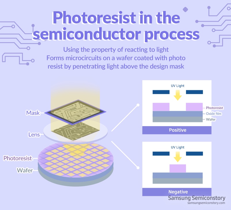
Wie wirken sich Alterungserscheinungen bei Photoresists aus? 18. A speed of about 500 rpm is commonly used during the dispensing step enabling the spread of the fluid over the substrate.Viele übersetzte Beispielsätze mit photoresist – Deutsch-Englisch Wörterbuch und Suchmaschine für Millionen von Deutsch-Übersetzungen.Photoresist They form circuit patterns on the surface of a silicon wafer with photochemical reaction caused by light irradiation through a photomask on which the circuit patterns are drawn. By introducing a UV sensitive compound . Enter a new target size for your image.
- Photovoltaik Leistungsoptimierer
- Piaggio Fürstenfeldbruck _ Traueranzeigen aus fürstenfeldbruck
- Phpmyadmin Delete Mysql , Delete all records in a table of MYSQL in phpMyAdmin
- Pick Up Original Shop | Dodge Ram Ersatzteilen
- Pharaoh A New Era Spiele _ Ein großer Aufbau-Klassiker kehrt endlich zurück!
- Pheromone Testberichte : Pheromonstecker Katze
- Pics Of Huge Spiders : 32 Vivid Red Spiders You May See (Pictures & Identification)
- Phone Number Spoofing – 5 best spoof call apps and fake call apps for Android
- Pickel Am Körper Im Gesicht – Akne-Karte: Was Unreinheiten im Gesicht über Ihre Organe aussagen
- Philips Rasierer Blade , Philips OneBlade Pro 360 Face + Body QP6541/15
- Physiotherapie Hausbesuche Karlsruhe
- Ph Wert Und Temperatur – pH-Wert
- Phonologische Bewusstheit Pädagogik