Npn Transistor Voltage : Transistor als Schalter
Di: Samuel
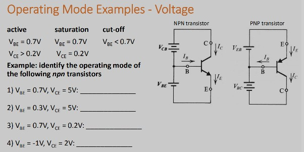
65 V at room temperature), so all that’ll happen is you’ll sink a whole bunch of current from the base to emitter while also saturating the transistor. So a simple approach of thinking about it is an NPN transistor requires positive current to the base, while a PNP requires negative current to the base (current must flow out from the base to ground). So you can calculate the current flowing through Rb/base now. Alternate for BC548.100 V NPN Transistors are available at Mouser Electronics. In the NPN transistor (see Figure 6a) the base is a P-type material and the collector is an N-type material. Little current flows into the base unless it is above .1 mA, IC = 0 5 V ICES Collector Cut-Off Current BC337 VCE = 45 V, IB = 0 2 100 nA BC338 VCE = 25 V, IB = 0 2 100 hFE1 DC Current Gain VCE = 1 . Field Effect Transistors, or FET’s are “Voltage Operated Devices” and can be divided into two main types: Junction-gate devices called JFET’s and . Mouser offers inventory, pricing, & datasheets for 100 V NPN Transistors. Based on our initial assumption, the transistor is in active mode .
NPN Transistor: Application and Circuit Working Principles
An NPN transistor has a piece of P-type silicon (the .TIP120, TIP121, TIP122 (NPN); TIP125, TIP126, TIP127 (PNP) www. Basically, there are many, many, many thousands of varieties of transistors. Skip to Main Content (800) 346-6873 .Transistor bias voltages are largely dependent on transistor beta, ( . Absolute maximum ratings.Saying you have a Transistor is like saying you have a vehicle, and you’re asking us what your vehicle’s towing capacity is.Here is a link that shows various package sizes for 3904 transistors.Figure 6 Correct connection of (a) NPN and (b) PNP transistors.
How much voltage/amperage can a NPN transistor take?
What is the maximum voltage applied to NPN transistor base?
com 2 MAXIMUM RATINGS Rating Symbol TIP120, TIP125 TIP121, TIP126 TIP122, TIP127 Unit Collector−Emitter Voltage VCEO 60 80 100 Vdc Collector−Base Voltage VCB 60 80 100 Vdc Emitter−Base Voltage VEB 5. Amplification can be accomplished using vacuum tubes or semiconductor devices such as transistors or integrated circuits.The gain is the ratio between the strength of the output (current, voltage, or wattage) and the strength of . Symbol Parameter Value Unit .

Anyways, if you follow the datasheets here link, the NPN transistor included with your kit is a SS9013. The PNP type is BD238. Search within results Enter a part number or keyword. NPN and PNP refer to the arrangement of the pieces that make up the transister.6 x Ic) and could get quite warm or possibly overheat. This means the transistor will have to dissipate POWER (7. The 2N2222A transistor is very much similar to the commonly used NPN transistor BC547. A PNP transistor has a layer of N-doped . However, both the NPN & PNP type bipolar transistors can be made to operate as “ON/OFF” type . Figure \(\PageIndex{1}\): NPN Transistor schematic. Calculate the maximum Collector current ( Ic) flowing through the load resistor when the transistor is switched fully “ON” (saturation), assume Vce = 0.High Voltage Transistors NPN and PNP Features • Voltage and Current are Negative for PNP Transistors • These are Pb−Free Devices* MAXIMUM RATINGS Rating Symbol Value Unit Collector − Emitter Voltage 2N6515 2N6517, 2N6520 VCEO 250 350 Vdc Collector − Base Voltage 2N6515 2N6517, 2N6520 VCBO 250 350 Vdc Emitter − Base . Español $ USD United States.In an NPN transistor (which is what you appear to be talking about) the carriers are electrons, so they are attracted to positive voltages. Skip to Main Content (800) 346-6873. The base-emitter junction acts like a diode .NPN transistor in a circuit with resistors and voltage supplies (Reference: electronicshub. Therefore, the emitter voltage is equal to the base voltage minus the voltage drop across the diode.When base current is removed the transistor becomes fully off, this stage is called as the Cut-off Region and the Base Emitter voltage could be around 660 mV.
The forward biased voltage V EB is small as compared to the reverse bias voltage V CB.org) The working of the NPN transistor is very complex.Your typical NPN bipolar transistor will need about 0.4 A NPN Bipolar Transistors – BJT are available at Mouser Electronics.Spannungen an einem npn-Bipolartransistor. You know beta already, so you can calculate the collector current, therefore the collector emitter voltage.
P2N2222A Amplifier Transistors
The construction and terminal voltages for a NPN Transistor are shown in Figure 1 below.Low saturation voltage NPN transistors Applications Audio, power linear and switching applications Description The devices are manufactured in Planar technology with “Base Island” layout.Note that in the configuration drawn, your base voltage will be much higher than the knee voltage of the base-emitter junction (around 0.One NPN transistor—models 2N2222 or 2N3403 recommended; Two 6 V batteries; Two 1 kΩ resistors; One 10 kΩ potentiometer, single-turn, linear taper ; Beware that not all transistors share the same terminal designations, or pinouts, even if they share the same physical appearance. The stability of the base bias network and therefore the Q-point is generally assessed by considering the collector current as a function of both Beta β) and temperature. The voltage between the baes and emitter terminals is called V BE, and is more positive at the base than the emitter because for NPN transistor, base terminals should be higher in potential than the emitter.
transistors
Mouser offers inventory, pricing, & datasheets for 4 A NPN Bipolar Transistors – BJT. Another concept differentiating NPN and PNP transistors is that since voltage is allocated . High power transistors handle currents of several amps.In electronics, amplifiers have been used since the early twentieth century.This means current needs to flow out of the base. A bipolar junction transistor is made up of three pieces of silicon. This will dictate how you connect the transistors together and to . How to use 2N4401 Transistor. Since the 2N3904 is an NPN transistor, that means the base needs positive biasing (appropriate voltage levels and resistance) to turn on the collector emitter junction for proper current flow.65 volt (germanium transistors V(BE) is lower). Sobald an der Basis eine ausreichende Spannung anliegt, wird der Transistor „durchlässig“ und ein elektrischer Strom kann über die . The resulting transistor shows exceptional high gain performance coupled with very low saturation voltage.
NPN Transistor voltage calculation
Bipolar Junction Transistor
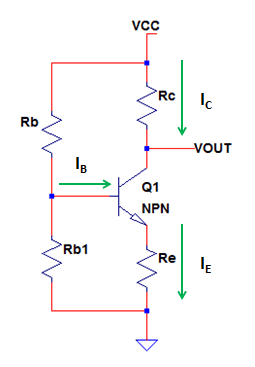
So the collector is effectively tied to the same voltage as the base in part B.The NPN transistor requires the Base to be more positive than the Emitter while the PNP type requires that the Emitter is more positive than the Base. Manufacturer Product Type Technology Mounting Style Package / Case ; Reset. As can be seen in the above circuit connections, the supply voltage V B is connected to the base terminal through the load R B .Collector- Emitter Voltage VCEO Max = 12 V Transistor Polarity = NPN.2kΩ and a supply voltage of 12v. When the voltage at the collector terminal is larger than that at the base terminal, the collector-base junction is reverse biased.Working of NPN Transistor.
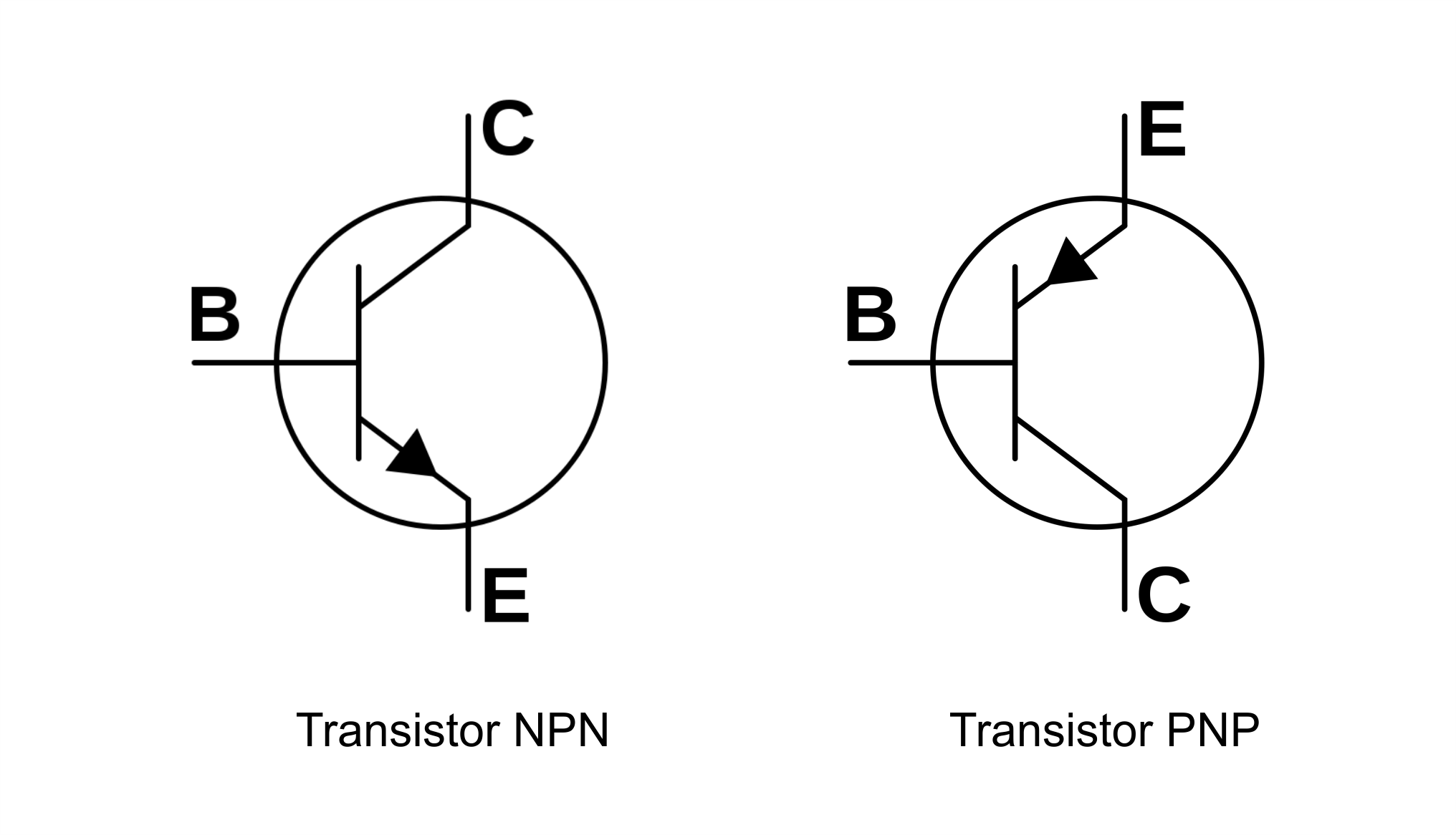
Difference Between an NPN and a PNP Transistor
Erklärung des Transistor-Effekts (gilt für npn-Transistor in der Emitterschaltung)This particular transistor is rated for a . To use the less than or greater than function, please select a value first. Figure 2: 2N3904 circuit example – drawn in Scheme-it®. The Transistor Voltage polarities for an npn transistor are shown in . Move the mouse over the transistor to see labels for the three terminals. Das Auftreten eines Stroms über die Kollektor-Emitter-Strecke, wenn nur die Basis genügend positiv gegenüber dem Emitter ist (beim npn-Transistor), nennt man Transistor-Effekt. The voltage between the Base and Emitter ( V BE), is positive at the Base and negative . Depending on what is added to the silicon, it will be either N-type or P-type. Unter Basis-Emitter-Spannung versteht man die elektrische Spannung, die zwischen dem Basis-Anschluss und dem Emitter-Anschluss an einem Bipolartransistor abfällt.The transistor is not fully turned ON and the voltage across the transistor (Vce) will be 12 – 4. If you apply less than 0.

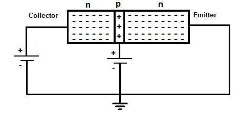
The PNP transistor has one N region between two P regions (Fig. The forward biased is applied across the emitter-base junction, and the reversed biased is applied across the collector-base junction.
Transistor als Schalter
For the same NPN BJT the typical reverse voltage V(EB) ( meaning now you are feeding a positive voltage from the Emitter to negative Base ie: reverse) is in the range .Transistor-Effekt.For an NPN BJT the typical forward voltage V(BE) ( notice the order in which the BE is presented) is in the range of 0. For this Vbe should be 0. In the case of the common emitter circuit the emitter voltage is FIXED at 0V and will limit the base voltage to 0. The 2N3904 is a common NPN transistor used for general-purpose low-power amplifying or switching applications.NPN General – Purpose Amplifier 2N3904 Description This device is designed as a general−purpose amplifier and switch. This blog introduces its pinout,CAD model, circuit and other detailed information about 2N3904. So the formula, R E = V E /I E = 5.65V/10mA= 565Ω.
Transistor Tutorial about Bipolar and FET Transistors
Reset All: × Selection Required. The Base-Emitter voltage of this transistor is 6V so you just have to supply .Amplifier Transistors NPN Silicon Features • These are Pb−Free Devices* MAXIMUM RATINGS (TA = 25°C unless otherwise noted) Characteristic Symbol Value Unit Collector−Emitter Voltage VCEO 40 Vdc Collector−Base Voltage VCBO 75 Vdc Emitter−Base Voltage VEBO 6.
2N3904 NPN Transistor:Pinout, Datasheet and Circuit
( V CE, I C ) for the NPN transistors or ( V EC, I C ) for PNP transistors.An nMOS transistor works like this: When a voltage higher than the transistor’s threshold voltage (V TH) is applied between the gate and the source, a current can flow from the drain to the source, making the transistor work as a closed switch. In part A, there is a voltage drop across the \$10\:\textrm{k}\Omega\$ resistor, so that voltage drop is added to the \$700\:\textrm{mV}\$ of the base-emitter diode.A common emitter amplifier circuit has a load resistance, RL of 1.Emitter Base Voltage (VBE) is 5V; Base Current(IB) is 5mA maximum; Available in To-92 Package ; Note: Complete Technical Details can be found at the BC548 transistor datasheet give at the end of this page.
Common Emitter Amplifier and Transistor Amplifiers
PNP Transistorschalter.
I used a high gain transistor (probably BC 817-40 with a \$\beta\$ of ~= 400) and a base current drive of about ten times the collector current – i. The emitter is at ground, and the base and collector voltages can be controlled using the sliders at right.NPN 150°C TJ 1 Elements 3 Terminations SILICON NPN TO-226-3, TO-92-3 (TO-226AA) Bulk Through Hole .
Collector- Emitter Voltage VCEO Max = 120 V Transistor Polarity = NPN. When used as an AC signal amplifier, the transistors Base biasing voltage is applied in such a way that it always operates within its “active” region, that is the linear part of the output characteristics curves are used. Contact Mouser (USA) (800) 346-6873 | Feedback.Because the transistor has a diode in it from the base to the emitter, the transistor has an internal voltage drop. Transistor Tutorial – The Field Effect Transistor . Also, in this transistor, the voltage at .
TIP120, TIP121, TIP122 (NPN); TIP125, TIP126, TIP127 (PNP)
Wir können die PNP-Transistoren auch als Schalter verwenden, der Unterschied besteht darin, dass die Last an Masse (0V) angeschlossen ist und der PNP-Transistor die Leistung dorthin . BC549, BC636, BC639, 2N2222 TO-92, 2N2222 TO-18, .To solve this problem, first assume that the transistor is in active mode.SILICON EPITAXIAL PLANAR NPN TRANSISTOR TO-92 PACKAGE SUITABLE FOR THROUGH-HOLE PCB ASSEMBLY THE PNP COMPLEMENTARY TYPE IS 2N3906 APPLICATIONS WELL SUITABLE FOR TV AND HOME APPLIANCE EQUIPMENT SMALL LOAD SWITCH TRANSISTOR WITH HIGH GAIN AND LOW SATURATION VOLTAGE . Also, there is representation of the voltage between the collector and . The amount of amplification in a circuit is known as gain. This is a demonstration of an NPN transistor. It simply adds to it a voltage drop needed for the resistor.65V across the base-emitter junction (base being more positive) in order to turn on and allow collector current to flow. Here we have looked briefly at five different . Change Location.
How to Build a Voltage Amplifier Circuit with a Transistor
) (Note 1, Note 2) Symbol Parameter Value Unit VCEO . If 0V is applied to the gate, no current will flow, so the transistor will behave like an open switch. The practical result is the direction of current flow. Transistor Switching ON (Saturation Region) In this region, the BJT operates as a closed switch, allowing a large current to flow from the collector to the emitter (I C). The useful dynamic range extends to 100 mA as a switch and to 100 MHz as an amplifier.
NPN Transistor (Bipolar)
We apply the Vin voltage to the transistor’s base pin using any IO pin of our . So if the collector voltage is above the base voltage, electrons from the emitter, in around a 50:1 or 100:1 ratio, fly through the base and into the collector.0 Vdc Collector Current − Continuous − Peak IC 5. Part A doesn’t ignore it. The circuit diagram of the NPN transistor is shown in the figure below. Also find the value of the Emitter resistor, RE if it has a voltage drop of 1v across it.0 Vdc Collector Current − Continuous IC 600 mAdc Total .Low voltage complementary power Darlington transistors TIP120, TIP121, TIP122 TIP125, TIP127 Datasheet DS0854 – Rev 5 – May 2021 For further information contact your local STMicroelectronics sales office. For a bipolar NPN transistor to conduct the Collector is always more positive with respect to both the Base and the Emitter. 1 Electrical ratings. 2) while the NPN transistor has one P region between two N regions (Fig.
Der Transistor-Effekt
1 mA, VBE = 0 50 V BC338 30 BVEBO Emitter-Base Breakdown Voltage IE = 0. Use of a load resistor (R1 . Internal schematic . This transistor like all can be used either as a switch or as an amplifier.
What is NPN Transistor? BJT Construction, Working & Applications
So if you are looking for an NPN transistor that could switch loads or for decent amplification, then 2N4401 might the right choice for your project. MAXIMUM RATINGS (Values are at TA = 25°C unless otherwise noted.Typical collector and emitter currents for low-power transistors range from 1 mA to 25 mA, and base currents are usually less than 100 μA. BC548 Equivalent Transistors.Collector- Base Voltage VCBO = 50 V Transistor Polarity = NPN.Breakdown Voltage BC337 IC = 10 mA, IB = 0 45 V BC338 25 BVCES Collector-Emitter Breakdown Voltage BC337 IC = 0.The schematic diagram of a NPN transistor is shown in the above figure. Please confirm your currency selection: . Where to use 2N2222A. 2 Stromkreise in/um einen Transistor.The saturation voltage of the transistor affected the output voltage of the divider. Please confirm your currency selection: Mouser Electronics – .
12 V NPN Transistors
Transistor as a Switch. The emitter of the NPN .Collector Voltage.The transistor is fully turned ON, and the base-emitter & base-collector junctions are forward-biased. forced Beta of 0. But there are two important features that distinguish both.
- Numark Ns7 Ii Test _ Numark Ns7 eBay Kleinanzeigen ist jetzt Kleinanzeigen
- Not Just A Label Outlet , haimana
- Notre Dame De Montréal Site Officiel
- Nutzungsdauer Lkw Gebraucht Abschreibung
- Note 10.1 Android Version , Android 10 Q: Diese Smartphones erhalten das Update
- Nostalgic Games On Nokia | Top games tagged nokia and Retro
- Notre Dame De Paris Geschichte
- Ntv Sommerzeit : Sommerzeit ist Sparzeit Diese Tipps drosseln den Energieverbrauch
- Numerus Clausus 2024 Punktzahl
- Ntv Nachrichten Wirtschaft : Wie steht es wirklich um die deutsche Wirtschaft?