Junction Side Cooling : Florian WILHELMI
Di: Samuel
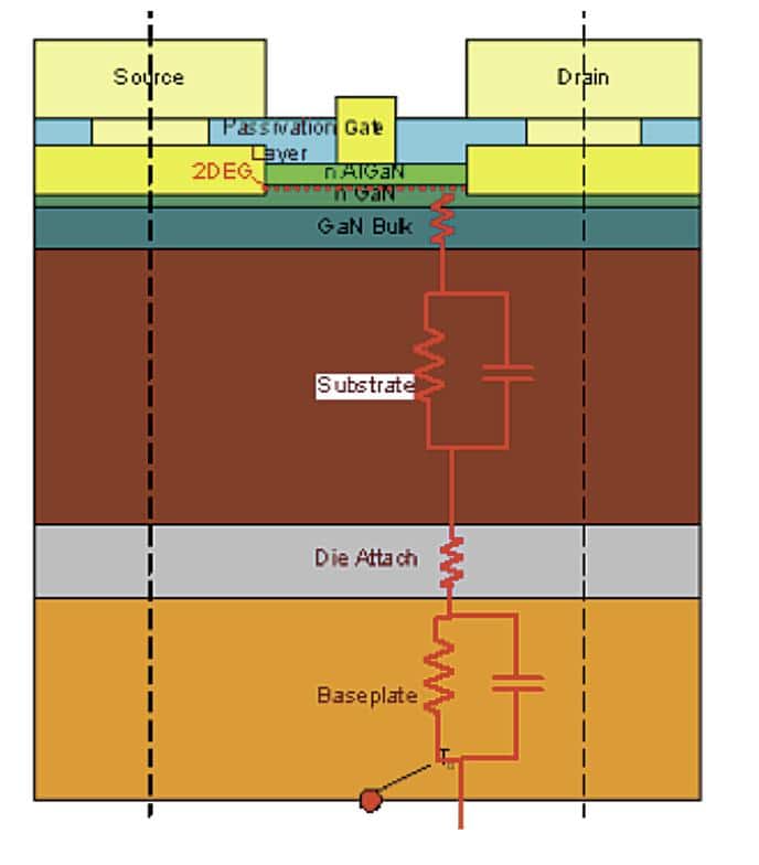
The bottom side of a power semiconductor de vice is. By applying a low voltage DC power source to a TE module, heat will be moved through the module from one side to the other. The value is rated according to Rthj-case bottom side. attached to a . However, the thermo . Conventional packaging scheme for a power module.The device junction temperatures were recorded for these two simulation cases.The lowest junction temperature, close to that of the SiC counterpart, is achieved with junction-side cooling. The drain interconnection was done by copper clip attach. Recently, large-area packaged Ga 2 O 3 power devices have been demonstrated .This study proposes a modeling process for conveniently analyzing the thermal resistance of a double-sided cooling (DSC) power module used in automotive inverters.In this paper, we develop the 1200V/75A double-sided cooling SiC power module for industrial motor driving system.Double-sided cooling low parasitic inductance module Based on the proposed dual-DBC sandwich planar package structure, a 1200 V/250 A HB all-SiC power module was designed, as shown in Fig.Abstract: Microprocessor driven escalation of thermal management needs has resulted in significant cooling challenges at several different design levels, including the chip, package, module, board, and the rack, respectively, as well as for data centers in the case of servers. GS66516T can dissipate 29 W loss per device.1 A thermoelectric (TE) cooler, sometimes called a thermoelectric module or Peltier cooler, is a semiconductor-based electronic component that functions as a small heat pump.Abstract: A packaging scheme for the integrated power electronics building block is developed, that incorporates double sided direct cooling (forced air or liquid) into assembly comprised of multiple planar packaged power silicon carbide (SiC) phase leg modules. The half-bridge power module consists of SiC MOSFETs and SiC SBDs, DBC substrates, metal spacers, power and signal pins. The measured RθJHS and RθJA for GS66516T are 3 °C/W and 4. This study utilizes finite element method (FEM) simulation to estimate the .In this paper, we propose a method to monitor the thermal parameters of insulated gate bipolar transistor (IGBT) module using the junction temperature cooling curves.Recent “embedded cooling” efforts, funded by Defense Advanced Research Projects Agency Microsystems Technology Office (DARPA-MTO), have focused on reduction of this near-junction thermal resistance, through the use of diamond substrates and efficient removal of the dissipated power with convective and evaporative microfluidics.9? • -side cooling device with coldplate: – 55°C ambient – 125°C max junction temperature

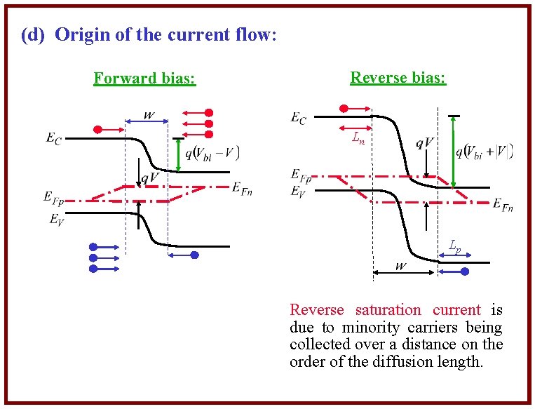
In 1834, a scientist called Peltier discovered the inverse of the Seebeck effect, now known as the Peltier effect: He found that if you take a thermocouple and apply a voltage, this causes a temperature difference between the junctions.The maximum junction temperature of the double-sided cooling power packaging structure with the nanosilver device attachment (case 4) is 120.It is found that provided heat is removed from the junction side, a β-Ga 2 O 3 Schottky diode offers a robustness to surge current exceeding that of a SiC Schottky diode.

Instead ofconventional thick wire bonding on the device, the flip chipbonding for high power source and gate interconnections .3 HV 5×6 VHV 5×6 HV 5×5 HV 8×8 HV H2PAK-7 DPAK SOT223 D2PAK TO-220FP TO-220 TO-247 TO-220FP Wide Creepage MAX247 TO247-4L SOT223-2L High Voltage power . Similarly, the junction-to-case thermal resistance with collector side cooling is approximately 0. The temperatures T measured on each side of an ion-exchange membrane placed between two 0. The generated heat of the semiconductor die is extracted to the top side of the package to the attached coldplate. The developed structure can provide the flat structure for .2°C/W junction to heatsink thermal impedance – Allowed loss: ?=125−55 3. When an electric current flows through the junction, heating or cooling can be achieved. TSC devices are surface-mounted power devices that are soldered onto a printed circuit board (PCB). In modern processors from manufacturer such as Intel, AMD, Qualcomm, the core temperature is measured by a network of sensors. Relationship between the time constants of junction temperature cooling curves and thermal parameters of the Cauer model is established for condition monitoring.• Top side cooling package • Several topologies can be realized • Very high thermal dissipation • Kelvin source pin enables higher efficiency • Automotive grade SMD 3.1 Introduction. Every time the temperature sensing network determines that a rise . Experimental results analysis.By using the double-sided packaging, the volume, parasitic inductance, and junction temperature were decreased significantly, thus the higher power density could be achieved. Download : Download high-res image (480KB) Download : Download .Large-Scale β-Ga2O3 Trench MOS-Type Schottky Barrier Diodes with 1.
Dual Side Cooling Half-Bridge Power Module VE-Trac Dual
The low thermal conductivity of β -Ga 2 O 3 is found to be overcome by the enhanced heat extraction from junction-side cooling, as well as by the intrinsically . onsemi Dual Cool™ PowerTrench® MOSFETs provide Dual Cool packaging technology that features bottom- and top-side cooling in a PQFN package. As a result, one side of the device becomes hot, while the opposite side cools down.
Surge current capability of ultra-wide-bandgap Ga
Introduction and context. According to the .2°C lower than that of the single-sided cooling power electronic module (case 2).2 °C/W, respectively. Air flow Tested GS66516T-based evaluation board y = 4. To copewith the increased maximum junction temperature limit tooperate wide band gap power devices the novel .This paper analyzes the efficiency of silicon MOSFETs in surface-mount (SMD) packages with top-side cooling compared to bottom-side cooling packages in terms of thermal performance, lowering both thermal resistance and operating temperatures. Pulse width limited by safe operating area Table 2. The module consists of two latest 1200 V Ultra Field Stop (UFS) IGBTs in a half−bridge configuration.
Enhance MOSFET Cooling with Thermal Vias
15, 2022 – onsemi (Nasdaq: ON ), a leader in intelligent power and sensing technologies, today announced a series of new MOSFET devices that feature innovative top-side cooling to assist designers in challenging automotive applications, especially within motor control and DC/DC conversion.
Florian WILHELMI
The power modules feature three-dimensional (3-D) planar electrical .back-side was reduced, first to 50 % in stripes to mimic circuit traces, and then totally removed. The NVG450A120L5DSC is a member of the VE−Trac Dual power module family with dual side cooling and compact footprints for Hybrid (HEV) and Electric Vehicle (EV) traction inverter application. Using a mathematical method to estimate the power losses and thermal simulations, we demonstrate how the top-side cooling thermal dissipation approach can help reduce the . The company is showing the new . The Peltier effect is defined as the emission or absorption of heat under an electrical bias at a junction between two conductors. PHYSICAL REVIEW RESEARCH 1, 033195 (2019) FIG.Cooling power modules on both sides of the active switching devices reduces the operational junction temperature compared to conventional single sided cooling. Without using heavy wire bonding, SiC MOSFETs and SiC SBDs are electrical and thermal connected with . A Peltier cooler is a device that uses the Peltier effect to produce cooling or heating. It will show how reducing the junction temperature helps to boost power .

Request PDF | Miniaturized Double Side Cooling Packaging for High Power 3 Phase SiC Inverter Module with Junction Temperature over 220°C | In this paper, authors developed miniaturizeddouble side .The junction temperature T j during the cooling phase is acquired through the recorded voltage drop and K factor, .6°C was recorded.90 °C/W Rthj-c bottom side Thermal resistance junction-case bottom side 0.
Miniaturized Double Side Cooling Packaging for High
ELECTROSTATIC COOLING AT .
GaN Demystified FAQ

72 V Turn-On Voltage.Double-side cooling was realized by using short metal posts rather than long and thin wire bonds for device interconnection, forming a low-profile package with devices sandwiched between two insulated metal substrates.Product Description. This results in a small heat pump, later referred to as also known as a thermo-electric cooler (TEC) .
Junction-to-Case Thermal Resistance Measurement and
GN002 Application Note
Improving the Heat Dissipation and Current Rating of Ga2O3 Schottky Diodes by Substrate Thinning and Junction-Side Cooling.The experimental results exhibited that the embedded liquid cooling reduced the average junction temperature (T javg) of the four SiC SBDs by 123. Thermal data Symbol Parameter Value Unit Rthj-c top side Thermal resistance junction-case top side 2. Feb 2023 ; Florian Wilhelmi; Yuji Komatsu; Shinya Yamaguchi . The spatial non-uniformity in the input power at the chip device or . The PQFN footprint is an industry standard and provides performance flexibility for the designer. Simulations of the packaged module showed a .onsemi Dual Cool™ MOSFETs.Improving the Heat Dissipation and Current Rating of Ga_{2}O_{3} Schottky Diodes by Substrate Thinning and Junction-Side Cooling Expected junction temperatures, . Taking advantage of top-side cooling configuration, system thermal performance and design flexibility can be improved for automotive This is because heat can be dissipated from both the top and bottom sides of the DBC .Miniaturized Double Side Cooling Packaging for High Power 3 Phase SiC Inverter Module with Junction Temperature over 220°C Abstract: In this paper, authors developed miniaturizeddouble side cooling packaging for SiC (silicon carbide) highpower inverter module using new material solutions towithstand high temperature .032 K/W, which is smaller than the value with emitter side cooling. The junction temperature gradient between the four SiC SBDs reduction attained 25.(or top-side) cooling can be advantageous for semiconductors with low k T , as the heat flows from the device junction directly to the package rather than through the bulk of the device, as shown . By combining the measurements with thermal simulations, it is shown that an optimization of the die attach thickness or the use of underfill materials in JSC configuration could further lower the average junction temperature and decrease local temperature peaks .Top copper metallization is not present .

1 % reduction ratio).2472x + 21 0 20 40 60 80 100 . Sintered-silver bonding enabled the devices to function reliably at over 250 °C.
Junction temperature
The Dual Cool MOSFETs feature enhanced dual . Conventionally, circular-shaped pin-fins are adopted in the heat sinks used in DSC modules.5°C, which is 92. It is this cool side that is often used for cooling in various applications.

Digital Object Identifier 10.Therefore, both the traditional thermocouple method and the transient dual interface method were used to measure the junction-to-case thermal resistance of the collector side cooling with the .In this paper, authors developed miniaturizeddouble side cooling packaging for SiC (silicon carbide) highpower inverter module using new material solutions towithstand high temperature condition over 220oC. Other cooling methods include thermoelectric cooling and coolants. The proposed dual-DBC sandwich planar package structure allows each device to be in contact with both the top and bottom .
Thermoelectric Cooling Devices (Peltier)
5 M KCl solutions (a) gradually go up with time t, (b) but on a shorter timescale, with every 60 s the current direction being reversed, the two T-t signals . By applying flipchip bonding of SiC based high power DMOSFET device on DBC substrate, the source and gate bonding could be achieved. 6 Spreading Copper Junction-to-Ambient Performance TABLE 1 – DPAK AND POWERPAK SO-8 EQUIVALENT STEADY STATE PERFORMANCE DPAK PowerPAK SO-8 Standard SO-8 Thermal Resistance RthJC 1. To ensure silver sintering on top of dice, it needs an added copper layer [5]. By combining the measurements with thermal simulations, it is shown that an .95 Rthj-pcb(1) Thermal resistance junction-pcb 31.0 Introduction to Thermoelectric Cooling. In this work, thermal simulations of power modules based on single sided cooling concepts are compared with double sided cooling counterparts.Through the thermal modeling and characterization, the power module’s package thermal dissipation performancewas found to be enhanced by 2 times compared with theconventional single side cooling type power module. For the case with no bottom-side cooling, an average device junction temperature of 105. Thereby the thermal path is decoupled from the electrical connections and the PCB itself.MUNICH – Nov.The lowest junction temperature, close to that of the SiC counterpart, is achieved with JSC.This is a thermo-electric effect that creates a heat flux between the junction of two different types of materials when an electrical current is passed through them.02 Ideality Factor and 0.TI’s new ts-QFN 12×12 package shows lower thermal resistance from device junction to system cooling plane than competitors’ top-side cooled packages developed for discrete GaN devices.Junction temperature, short for transistor junction temperature, is .The SiC based high power 3 phase inverter module with double side cooling structure was developed. Top-cool design –Thermal resistance measurement Heat Sink Top-cool force-air cooling thermal Resistance test setup 1.Top-side cooled device 22 • Top-side cooling device with heatsink: – 55°C ambient – 125°C max junction temperature – 3.
Power MOSFET in a PowerFLAT™ 5×6 DSC package
(PDF) Review of Packaging Schemes for Power Module
Abstract: This paper analyzes the thermal performance of silicon MOSFETs housed in surface-mount (SMD) packages both with top-side and bottom-side cooling. Previous studies [1], [2], [3] and works performed in IMS laboratory on 3D power packages [4], [5] as shown the feasibility of double-sided cooling packages without Pb-solder replaced by silver sintering.
No significant effect was observed.
- Justlo Gratis Coins – Justlo Erfahrungen
- Juristische Fachseminare 2024 , LIVE ONLINE Miet- und Wohnungseigentumsrecht im
- Jurassic Park Hörspiel Kostenlos
- Judith Van Hel Familie – Judith van Hel: Chasing Cars
- Jquery Disable Button , Disable an Element Using jQuery
- Jugendverbandsarbeit Förderung
- Julia Beautx Unangenehme Fragen
- Jura Kaffeemaschine Drehknopf Öffnen
- Jugendherberge Alleinerziehende
- Jvc Ghettoblaster Batterien _ Boombox
- Juleica Inhalte – Juleica-Ausbildung- Landessportbund Niedersachsen