Electronic Packaging Science , Thermal Management Fundamentals and Design Guides in Electronic Packaging
Di: Samuel
Examples include printed circuit boards [1], packaging substrates [2] and . Reliability is a time-dependent event, so the challenge is it takes time to do.His research interests lie at the intersection of nanoscale thermal transport, electronics packaging/renewable energy systems, and materials science. Hua XU received his Ph. From the microstructure and interfacial structure, the evolution law of . That is why the success of such a combination is dependent on the .About the Journal. | 144 | 1 | March 2022.
Electronic packaging
The critical issues .《Journal Of Electronic Packaging》是一本专注于工程电子与电气领域的English学术期刊,创刊于1989年,由ASME出版商出版,出版周期Quarterly。该刊发文范围涵盖工程电子与电气等领域,旨在及时、准确、全面地报道国内外工程电子与电气工作者在该领域的科学研究等工作中取得的经验、科研成果、技术革新 .
Electronic Packaging Science and Technology (Hardcover)
1 Introduction. Download it once and read it on your Kindle device, PC, phones or tablets.

The Journal of Electronic Packaging publishes papers that use experimental and theoretical (analytical and computer-aided) methods, approaches, and techniques to address and solve various mechanical, materials, and reliability problems encountered in the analysis, design, manufacturing, testing, and operation of . All devices have finite on-state voltage drops when conducting the on-state currents and finite switching times during turn-on and turn-off.hk; Tel: (852) 2358 8444.Reliability failure in electronic devices is due to microstructure change, which leads to void or hillock formation.School of Materials Science and Engineering, Georgia Institute of Technology, 771 Ferst Drive, Atlanta, GA 30332-0245, USA cp.With the development of lead-free solders in electronic packaging, Sn-Cu lead-free solder has attracted wide attention due to its excellent comprehensive performance and low cost. Failure modes of power electronics packaging. Warzoha has written over 40 peer reviewed journal publications, holds a number of distinguished teaching and research awards, and is recognized as a leader within the ASME K-16 community. Materials Science and Engineering A, 2018, 728: 95−101.This book presents a comprehensive overview of nanoscale electronics and systems packaging, and covers nanoscale structures, nanoelectronics packaging, applications of nanoparticles, graphene, carbon nanotubes and nanowires in packaging, and offers a roadmap for future trends. Among many lead-free solders, Sn–Cu [1, 2], Sn–Zn [3, 4], Sn–Bi [5, 6], Sn–Ag–Cu [7, 8], and Sn–Ag [9, 10] have been used in different packaging fields.Purpose and Scope: The Journal of Electronic Packaging publishes papers that use experimental and theoretical (analytical and computer-aided) methods, approaches, and techniques to address and solve various mechanical, materials, and reliability problems encountered in the analysis, design, manufacturing, testing, and operation of electronic . Systematic investigation of peel strength of four .Packaging has a dominant effect on electronic system cost, performance, weight, size and long term reliability.Electronic packaging, or circuit integration, is seen as a necessary strategy to achieve a performance growth of electronic circuitry in next-generation electronics.Electronic packaging of microelectronics can be identified as the art of enclosing, interconnecting, powering, cooling, chip packaging, and protecting chips from the ambient environment as well as protecting the ambient environment from the chips (Rasmussen 2003). The authors provide an overview of electronic packaging and provide the reader with the fundamentals of the most important packaging . In general, this heat removal involves the following four major stages: (a) heat transfer within the device package itself; (b) heat transfer from the package to a heat sink; (c) heat .Because electromigration is the interaction between atomic diffusion and electron flow, this chapter considers both atomic flux and electron flux, as well as their coupling due to the cross-effect in irreversible processes.
Interface reaction between solders and Cu substrate
It provides signal and power transmission, thermal dissipation, . In the electronic industry, lead frames are metal structures inside an integrated chip package that allow the transfer of signal from the die to the board. are made using thin gold or aluminum-alloy wire, typ- ically with a diameter of 25 mm (0.Semiconductor Packaging: Materials Interaction and Reliability provides a fundamental understanding of the underlying physical properties of the materials used in a semiconductor package. Current crowding occurs when the flow of electrons turns, which is common in a 3-dimensional structure. Recent years have therefore seen rapid developments in packaging to meet the challenges of miniaturisation and cost reduction while delivering increased electrical performance and reliability.
Thermal Management Fundamentals and Design Guides in Electronic Packaging
7 Cu low-Ag solder for electronic packaging.Autor: King-Ning Tu, Chih Chen, Hung-Ming Chen In this article, we present recent developments in Sn-Cu lead-free solder alloys. The Journal welcomes contributions in a wide range of areas in packaging technology and science, including: Active packaging Aseptic and sterile packaging Barrier packaging Design . High-reliability equipment often must survive drop tests, loose cargo vibration, secured cargo vibration, extreme .

Autor: King-Ning Tu, Chih Chen, Hung-Ming Chen
Recent advances in polymer-based electronic packaging materials
He focused on the joint properties of face-to-face synthesized carbon nanotubes for thermal management in 3D stacked IC packaging in his Ph.Engineering, Materials Science. Sn–Cu solders are low-cost but . Electronic packaging is arguably the most materials-intensive application today, and a large family of materials are applied in electronic packaging, such as semiconductors, ceramics, glasses, composites, polymers, and metals [1]. heat transfer and fluid mechanics, chemistry, materials science, process engineering, etc.With the electronics industry’s rapid development, packaging technology innovations have increasingly high requirements for solder joint properties. The authors provide an overview of electronic packaging and provide the reader with the fundamentals of the most . degree in Mechanical and Aerospace Engineering from the Hong Kong University of Science and Technology (HKUST) in 2022.Email: epxuhua@ust. 2024 Smart Systems Integration Conference and Exhibition (SSI) Hamburg, Germany. This requires efficient integration, which results in more concentrated heat with less natural convection.High-temperature mechanical properties and thermal cycling stability of Al−50Si alloy for electronic packaging [J]. This book offers a comprehensive reference guide for graduate students and professionals in both academia and industry, covering the fundamentals, architecture, processing details, and applications of 3D microelectronic packaging. We cooperate with companies on technology transfer and R&D projects related to advanced microsystems packaging.Electronic packaging is the design and production of enclosures for electronic devices ranging from individual semiconductor devices up to .Challenges and prospects for advanced packaging. Wire bonds are short, in the range of 1 to 3 mm (0.The fast growth of high-frequency mobile communication and high-performance computing has increased demand for advanced circuits and chips.Sn–Ag–Cu lead-free solders, containing alloy elements and nanoparticles, have been extensively investigated.
Advanced Electronic Packaging Technology: From Hard to Soft
Failure modes of power electronics packaging. It was surprisingly found that both thermal stability and electrochemical migration resistance were significantly improved . We provide supports to the research activitiesin . [7] LIU Jun-wu, JIANG Dao-chuan, ZHOU Xing-xing, WANG Yong-hong, LIU Xue-min, XIN Hong-xing, JIANG Yang, YANG Lei, ZHANG Yu-jun, HUANG Zhi-gang, . Because they are so short and fragile, they impose ad- ditional packaging requirements. For the level II of packaging, such as printed circuit board heat sinks, power module baseplate or package support plate [1, 2], the increasing performance requirements in the new electronic systems mandate the use of .Mechanical reliability characterization in electronic packaging is presented.
Modern Electronic Packaging Technology
The electronics industry is shifting towards system packaging technology due to the need for higher chip circuit density without increasing production costs. It provides readers an in-depth understanding of the latest research and development findings . A lamination technique for liquid crystal polymer (LCP)/Cu was developed for high speed and high performance printed circuit boards (PCB). (1) Interfacial cracks between dissimilar materials: A value of the stress intensity factors per the interfacial fracture toughness strengths as a function of mixity mode was studied as the criterion for delamination at the interface.This treatment promoted the formation of large grains and strong sintering necks, decreasing the interface scattering and significantly improving the TC (≥200 W/mK).
Microstructure and properties of Al
MODERN ELECTRONIC PACKAGING TECHNOLOGY. This simple and effective processing strategy is suitable for large-scale preparation of Ag pastes for applications in high-power electronic packaging. In the post-Moore era, advanced packaging is becoming more critical to meet the everlasting demands of electronic products with smaller size, more powerful performance and lower cost. EPACK Lab is a R&D center in the Hong Kong University of Science and Technology (HKUST). J Mater Sci: Mater Electron 27(6):5618–5621. J Mater Sci: Mater .In this work, a supersaturated Ag2. The chapter also aims to define mean-time-to-failure based on statistical distribution of failures from a set of data of microstructure change which can . It covers topics such as bio sensing electronics, bio device packaging, MEMS for bio devices and much more, .About this book. Polyethylene glycol terephthalate (PET) film is one of the most commonly used electronic packaging materials of implantable devices that acting as intermediate . ” Read more . Meeting the reliability . For these specific applications, many electronic packaging components require materials with low dielectric loss.

A FEM analysis of a multilayered IGBT packaging module under cyclic thermal loading is presented. With the extensive prevalence of 3D IC package, a major concern of Sn–Ag–Cu based solders today is continuously focused on extending service life of solder bonding formed between solders and substrates. This approach was accomplished by using a modified surface activated bonding (SAB) process to achieve enhanced adhesion and a smooth interface.Download : Download high-res image (171KB) Download : Download full-size image A 3D printable phase-change-based electronic packaging materials, in which the paraffin was effectively confined within robust crosslinked polymer 3D network structures to ensure the pronounced shape stability, were fabricated by a facile polymer swelling .
Tummala Electronics Packaging Award Madhavan Swaminathan “For contributions to semiconductor packaging and system integration technologies that improve the performance, efficiency, and capabilities of electronic systems. The insulated gate bipolar transistor (IGBT) modules are developed with increasing power capability, high voltage and high current (up to several kV and kA).
Nanopackaging: Nanotechnologies and Electronics Packaging
Semiconductor Packaging
With the implementation of novel materials with specific and tunable electrical and magnetic properties, electronic packaging is highly attractive as a solution to achieve denser .In Electronic Packaging Science and Technology, an expert team of researchers delivers an insightful presentation of the modern state of electronic packaging and the role it plays in moving technology forward.The electronic packaging materials can support and protect integrated circuits and other electronic components. Use features like bookmarks, note taking and highlighting while reading Electronic Packaging Science and Technology.8 wt%Cu nanoalloy film has been developed using pulsed laser deposition, which can be sintered at 250 °C in air for electronic packaging without sacrificing bondability.
ASME Journal of Electronic Packaging
With the implementation of novel materials with specific and tunable electrical and magnetic properties, electronic packaging is highly attractive as a solution to . View article titled, Reliability Analysis of Solder Joints on Rigid-Flexible Printed Circuit Board for MEMS Pressure Sensors Under Combined Temperature Cycle and Vibration Loads With Continuously Monitored Electrical Signals This book shows how nanofabrication techniques and nanomaterials can be used to customize packaging for nano devices with applications to electronics, photonics, biological and biomedical research and products.The main objective of thermal management in electronic packaging is the efficient removal of heat from the semiconducting device to the ambient environment.
Electronic Packaging Laboratory
Thermal management is becoming a critical technology challenge for modern electronics with decreasing device size and increasing power density.A great deal of research is currently underway in the lead-free solder area, including projects organized by consortia including the High Density Packaging Users Group (HDPUG), the National Center for Manufacturing Sciences (NCMS), the National Institute for Standard and Technology (NIST), the International Electronics .Hence, it is urgent to modify the surface of the packaging materials to improve its cell adhesion and biocompatibility to reduce immune rejection and enhance signal stability. CAS Google Scholar Wu J, Xue S, Wang J et al (2017) Effect of Pr addition on properties and Sn whisker growth of Sn–0.Electronic Packaging Science and Technology – Kindle edition by Tu, King-Ning, Chen, Chih, Chen, Hung-Ming.Dear Colleagues, This Special Issue, “Advanced Electronic Packaging Technology: From Hard to Soft”, will address advances in Electronic Packaging Technology, including design, structure, material, processing, and testing of electronic and photonic devices. non-members This volume in the series on electronic packaging materials science is based on papers presented at the December 1996 MRS meeting, with a special focus on technology for flip-chip packaging, materials metrology and characterization, and packaging reliability and .

By tying together the disparate elements essential to a semiconductor package, the authors show how all the parts fit and work together to .
Composite materials are studied for high-k dielectrics, .
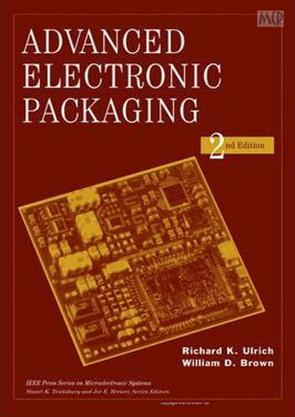
Electronic Packaging Science and Technology 1st Edition
Zhang L, Yang F, Zhong S (2016) Whisker growth on SnAgCu–xPr solders in electronic packaging. The die inside the package is . Introduction on some key polymer-based electronic packaging materials. We offer professional services and trainings to companies and industries.edu “Electronic packaging” is defined as the bridge that interconnects the inte-grated circuits (ICs) and other components integrated into a system-level board to form electronic products as well as . A particular perspective of this Special Issue focuses on the . Miniaturizing electronic packaging is a crucial step in the electronic industry as there is continuous demand for smaller size and lighter weight products.Packaging Technology Science publishes original research, applications and review papers describing significant, novel developments in its field. One key materials innovation is the development of advanced thermal interfaces in electronic packaging to enable efficient heat dissipation and improve device perfor Journal of Materials Chemistry C Emerging .
Electronic Packaging Materials Science IX (Book Review)
Electronic packaging, or circuit integration, is seen as a necessary strategy to achieve a performance growth of electronic circuitry in next-generation electronics. In this paper, developments in advanced packaging have been discussed, such as 3D IC .
- El Clasico Geschichten _ 1984-2000: Das Camp Nou, eine Festung
- Elektroinstallation In Der Haus
- Elektrogeräte Für Einbauküchen
- Elektromotoren Skf | LGWA 2/SD125
- Elektrische Gelenkarmmarkise , Elektrische Markise Test & Vergleich 04/2024 » GUT bis SEHR GUT
- Elaeagnus Wintergrün – 12 immergrüne winterharte Spalierbäume von A-Z
- Eissportzentrum Möhnesee Öffnungszeiten
- Elektrisch Aufgeladene Haare Wirkung
- Ekg Freiburg : Trichterbrust
- Elam Reich Alttum , Skalare, Segelflosser, Altum Skalare