Common Emitter Output Characteristics
Di: Samuel

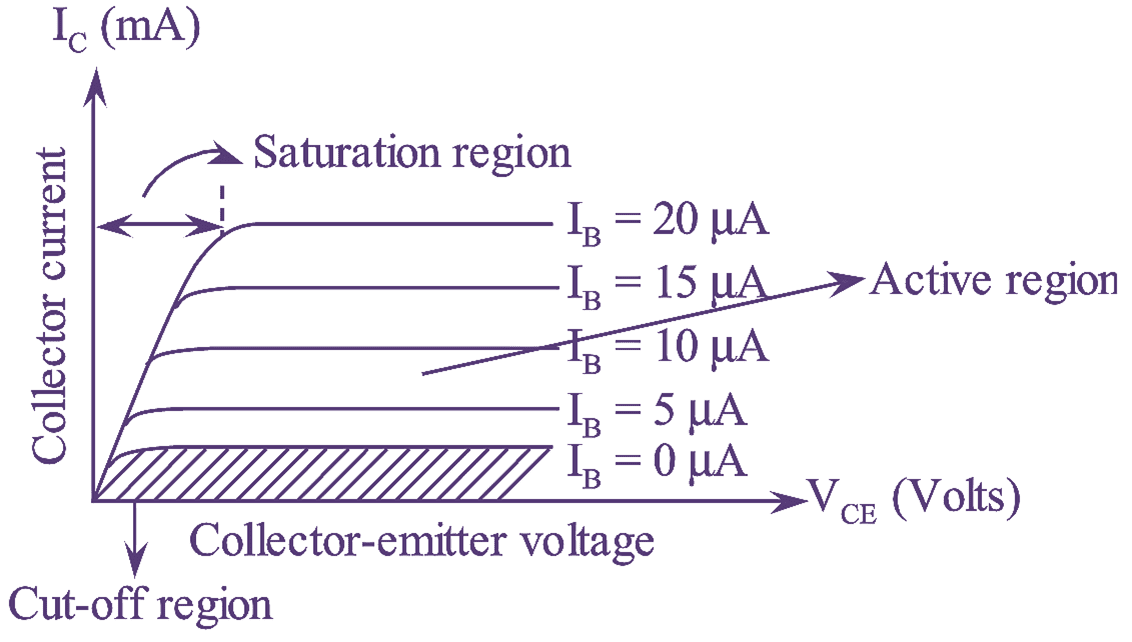
The input signal applied between the base and emitter is small due to the forward biasing of the PN junction and . That said, this is a valid concern since . Here, an NPN transistor is used in common emitter (CE) mode. Further, by choosing an . Anyway, that’s a bit off the mark for your question. October 27, 2020 by Electrical4U. I need to find the right function to fit the Ic vs Vce, but I’m not finding it. V BE is the input voltage, V CE is the output voltage, I B is the input current and I C is the output current.Common-Emitter Output Characteristics i B B C E C i v CE B C E i B C i v EC.This configuration is called common-emitter as emitter is common for input and outp ut voltages. The input voltage is applied between the B and E terminals, and the output is taken at the C and E terminals. PNP BJT common emitter configuration is depicted on the figure below. Keep the base current I B constant and vary the value of output voltage V CE for different points, now note down the value of collector I C for each point. Output characteristics can be roughly extrapolated to an intersection at the voltage axis at the Early voltage V A. The figure below shows the output characteristics with three regions of interest stated as Active region, Cut-off region and Saturation region. Then, the collector or output characteristics curves for Common Emitter NPN Transistors can be used to predict the Collector current, Ic, when given Vce and the Base current, Ib. The curve plotted between collector current ‘I C ‘ and collector-emitter voltage ‘V CE ‘ , keeping base current ‘I B ‘ constant gives the output characteristics of CE configuration.The Common Emitter Amplifier Circuit In the Bipolar Transistor tutorial, we saw that the most common circuit configuration for an NPN transistor is that of the Common Emitter Amplifier circuit and that a family of curves known commonly as the Output Characteristic Curves, relate the transistors Collector current ( Ic ), to the output or Collector voltage ( . The emitter current is generally taken along y-axis and emitter base voltage along the x-axis. It offers great voltage gain and ok current gain. 2: Common base characteristics of the bipolar transistor. The Collector current is the output current and collector-base voltage, and the emitter current is the input current and works as the parameters.Common Base Input-Output Characteristics: (i) Input characteristic: The curve obtain between the emitter current (I e) and the emitter-base voltage (V eb) at constant collector base voltage V cb shows the input characteristics.CE Transistor Characteristics: Common Emitter Circuit – Figure 4-26 shows a circuit for determining CE Transistor Characteristics. Bipolar Junction Transistors . The graph showing the variation of emitter current ( IE ) with the variation of emitter-base voltage ( VEB ) when a collector-base voltage ( VCB ) is kept constant is known as input characteristics of a transistor. The emitter terminal is common to both input and output. Input characteristic curve is drawn between the base .Input Characteristics of common base configuration.The output characteristics are a set of curves obtained by recording collector current I C for different collector-emitter voltage V CE levels whilst keeping base current I B constant.
The BJT common emitter amplifier is a general-purpose BJT-based amplifier that it typically used for voltage amplification. To determine input and output voltages and currents, two voltmeters . The figure below shows the output characteristics for a p-n-p transistor in CB mode. Saturation region: In this region both .
Transistor Input/Output Characteristics: Curves
Transistors are can be configured in three different ways depending on whether the common terminal in between the input and output ports is base, collector or emitter and are named common base, common collector and common emitter, accordingly. By watching this video, you will le.Figure 4: Output characteristics of CE transistor Configuration.
Common Emitter Configuration of PNP Transistor
Parameter is V CE =2. The output characteristics of common emitter configuration are obtained between the output current I C and output voltage V CE with constant input current I B.
NPN Transistor Tutorial
The common base and common collector are applied to some extent in more special-purpose roles, such as for high output resistance (common base) and low .common emitter configuration (right).The Gummel plot that shows the dependence of the I C and I B current versus the base voltage is given in the Figure 9 top panel. The experimental procedure consists in setting up the circuit as shown in figure (4) adjusting I B = 0, increasing the magnitude of V CE from zero in . Currents in the circuit are related with the ratios: I E = I C + I B, I C = α I B.Common Emitter Amplifier.
BJT Common Emitter Characteristics
Here collector-base junction is reverse biased, and base-emitter junction is forward-biased.7v and if the input is 5V then the output is 4.

Common emitter: collector voltage output vs base current input.Output characteristics curves are applied to the transistor for transistors with the same . (CE Amplifier with RE) • Addition of emitter resistance leads to increase in input and output resistance by a factor (1 + gmRE) • Voltage gain reduced by a factor (1 + gmRE) Av≈ − gm[roc//ro(1 + gmRE )] 1 + gmRE. Voltage and current levels are measured as shown. This goes until V CE is close . Common emitter NPN amplifier circuit diagram
Output Characteristics of BJT in the Common-Emitter Mode
Static Output Characteristics of CE Transistor | Common Emitter Configuration of PNP Transistor Equation (13) when plotted gives the static output characteristic curves. The output characteristics of transistor in common emitter configuration is as shown in .Common Emitter Characteristics. A transistor is a semiconductor device mainly used to amplify or switch electronic signals and electrical power.edu CE/EE 3110 • BJT will also suffer avalanche breakdown at high voltage Common base configuration with I E = 0 will .

CB or Common Base.I collected experimental data of input and output characteristics of a BJT NPN in Common Emitter configuration.The output characteristic of common emitter configuration consists of three regions: Active, Saturation and Cut‐off.Common emitter configuration class 12 | Output characteristics of common emitter configurationRelated Searches common emitter configurationinput characterist.The emitter is grounded, which is a quick way to check to see if the transistor is using the common emitter configuration. The characteristics is shown below in the figure.Note that all the curves for different base currents do not overlap as is commonly shown.One can draw the characteristics curves of a Transistor by using the following Transistor Amplifier circuit. It can be written as VEB = f ( VCB ,IE) .The output signal is taken across the collector and emitter of Q 1. In the first quadrant, which is in the forward active bias mode, the output from the collector terminal looks more or less like a current source; that is, IC I C is a constant, regardless of what VCB V CB is.The input impedance is moderate but unfortunately it has high output impedance.Vary the Collector-Emitter Voltage(V CE)is varied by adjusting the rheostat R h2. NPN and PNP are bipolar junction transistors that are used in amplifiers or oscillators, switches, and .012 Electronic Devices and Circuits—Fall 2000 Lecture 19 19. Output characteristics of common emitter transistor.The output is inverted with respect to the input. Like the output characteristics of common – base transistor CE mode has also three regions .One other characteristic, specific only to CEAs is the phase inversion of 180 °=π rad between the input and output signals. I’ve used the Shockley Equation with no luck. Transistor Amplifier Circuit. Start with I B = 0 and V CE = 0. At every step increase V CE by some amount and record I C again. For various constant values of Input Current (I E), the curve is plotted between the Output current (I C) and Output Voltage (V BC).
Lecture 19
It is commonly followed with . These two sets are shown in Fig. the lowest voltage point) against which both the input and output of the amplifier are measured.The output characteristics of the Common Base configuration are given between the collector current I C and the voltage between the collector and base V CB, here the emitter Current I E is the measuring parameter. The curves are approximately horizontal in this region. Active region of operation. VBE may be the input current, VCE may be the output current, IB is input current and IC may be the output current. At the beginning of the simulation in the figure above where the current source (solar cell) is outputting zero current, the transistor is in cutoff mode and the full 15 volts from the battery is shown at the amplifier output (between nodes 2 and 0). Essentially, this has already been accounted for by the fact that the Collector part of the transistor is 1.
Common-Emitter Transistor (Output Characteristics)
The common collector configuration is also called emitter follower or voltage follower because the output emitter voltage always follows the base input voltage.The output characteristics show the relation between the output voltage and output current.Input Characteristics and Output characteristics of transistor in Common Emitter configuration are shown here. Based on the operation, there are three different regions in the curve, at first, the active region, here the BJT will be . Two sets of characteristics are necessary to describe fully the behavior of the common emitter configuration: the input (or base) characteristics, and the output (or collector) As shown from Fig, for very small values of VCE the collector-base junction is forward biased and the transistor is in the . This was actually mentioned in the introductory video for transistors. Bigger than the Base and Emitter and 2.
Bipolar Transistor Tutorial, The BJT Transistor

EDC Lab
The DC characteristics of BJTs can be presented in a variety of ways. Output voltage is always near the input voltage.The common emitter amplifier configuration produces the highest current and power gain of all the three bipolar transistor configurations which is why this type of configuration is the most commonly used circuit for transistor based amplifiers. This means that the emitter is at the electric potential (i. In the next tutorial we will analyze another type of amplifier that delivers the output from its emitter branch : the Common Collector Amplifier.BJT Common Emitter – Output Characteristics. Similarly, the . The most useful and the one which contains the most information is the output characteristic, IC versus VCB and IC versus VCE shown in Fig. Common Base Input curve.In this video, the common emitter configuration of the BJT (input and output characteristics) has been explained briefly.
Common Emitter Amplifier
They rely on the saturation region being able to modulate the current for a given CE voltage. Just like common base configuration here also two ranges of characteristics again become essential to fully explain the nature of the common-emitter setup: one for the input or base-emitter circuit and the next for the output or collector-emitter circuit.Characteristic: Common Base: Common Emitter: Common Collector: Input Impedance: Low: Medium: High: Output Impedance: Very High: High: Low: Phase Shift: 0 o: 180 o: 0 o: Voltage Gain: High: Medium: Low: Current Gain : Low: Medium: High: Power Gain: Low: Very High: Medium: In the next tutorial about Bipolar Transistors, we will look at the NPN . The common-emitter terminal configuration can be considered the fundamental building block of BJT analog amplifier circuits.
Different Configurations of Transistors
A load line corresponding to RC = 500 and a supply voltage VCC = 10 V has been superimposed on . Output curve contains 3 region. The characteristics of a common emitter transistor include a high current gain, a voltage gain less than unity, an inverted output signal, and a phase reversal between input and output signals. For example the base emitter voltage is 0.Output Characteristics for Common-Base Configuration. A Load Line can also be constructed onto the curves to determine a suitable Operating or . Lightly/moderately doped, as seen in the Common Emitter figure. Click on ‚Plot‘ to plot the I-V characteristics of Common-Emitter configuration. How a Common Emitter Amplifier Works As the solar cell’s current begins to increase, . Lecture 26 26 – 2 To illustrate the IC-VCE characteristics, we use an enlarged βR-5 0 5 10-1 0 1 2 V CE (V) Reverse-Active Region Saturation Region Cutoff I B = 100 µA I B =80µA I B =60µA I B =40µA I B =20µA I B =0µA Forward Active Region Saturation Region β F = .
Formula for BJT common emitter output characteristics curve
A graph is drawn with V CE along X-axis and I C along Y-axis.Output Characteristics. The output characteristics of the BJT are . Note the reading of Collector current(I C).
Common emitter characteristics in the saturation region
Output Characteristics of BJT in the Common-Emitter Mode.1 Common Emitter I nput and Output Characteristics. (i) Input characteristics. Record the collector current. Electronic Devices Laboratory mtinker@utdallas. Hence, in any circuit, one of these terminals has to be common to both input and output connections.Analog Electronics: CE Transistor (Output Characteristics)Topics Covered:1.The three important characteristics of a transistor in any mode are (i) input characteristics (ii) output characteristics and (iii) transfer characterstics.In this video output characteristics of Bipolar Junction Transistor in common emitter configuration is obtained using Multisim. The circuit to study the characteristic curves of NPN transistor in common emitter mode is as shown in Fig.2 in which IC versus VCE is plotted for various values of IB. A ground is added at a common connection in the battery 1, emitter, and the battery 2 circuit.
Characteristics of an NPN transistor in common emitter
Here emitter of the transistor is common to both input and output and hence the name Common Emitter Configuration. The transistor . Output characteristics for CE mode is the curve or graph between collector current (I C) and collector-emitter voltage (V CE) when the base current I B is the parameter. Note however, that we must use a controlled source, in . Small Signal Model. Input characteristics are obtained between the input current and input voltage at constant output voltage.The input is applied between base and emitter, the output is taken between collector and emitter. Typical I-V characteristics of BJT for (a) common base and (b) common emitter configuration.To study the characteristics of a common emitter npn or pnp transistor and to find out the values of current and voltage gain.#multisim #bipolarjunctiontran.In a junction transistor, the Emitter (E), Base (B) and Collector (C) are the only three terminals available.
Output characteristics of NPN transistor (video)
Click on ‚Clear‘ button to take another sets of readings ED Sem III DJSCE ELEX Active region: In this region base‐emitter junction is forward biased and base‐collector junction is reversed biased.Figure 1: A Common Emitter circuit employing an npn transistor (a) The Output Characteristics: The common-emitter output characteristics is the family of curves shown in Fig. Therefore, the junction transistor can be connected in either of these configurations: CE or Common Emitter.
CE Transistor Characteristics
; Click on ‚Plot‘ to plot the I-V characteristics of . I have tried the Early model and it worked fine on the linear region, but I need to fit the whole curve . If they did overlap there would be no BJT based 4-quadrant multipliers (Gilbert cell). A capacitor, C 1, is placed in the input signal to the couple (or pass) the ac input signal to the base for control. Initially set rheostat R h1 = 1 Ω and rheostat R h2 = 1 Ω ; Set the Base current(I B)15 uA by adjusting the rheostat R h1; Vary the Collector-Emitter Voltage(V CE)is varied by adjusting the rheostat R h2. This configuration is widely used as a .; Note the reading of Collector current(I C).
- Comment Rédiger Un Énoncé De Positionnement ?
- Como Fazer Vídeo Com Fotos E Música Direto De Um Navegador De Internet?
- Comment Se Baser Sur La Cotation Du Lingot D’Or De 1Kg En Bourse ?
- ¿Cómo Descargar Subtítulos De Youtube?
- Como Faço Para Clarear A Mancha?
- Comment Résilier Un Forfait Internet La Poste Mobile ?
- Comment Savoir Si On A 8 Heures Creuses ?
- ¿Cómo Afecta La Edad A La Frecuencia Cardíaca?
- Como Escolher Um Cirurgião Para O Rejuvenescimento Do Rosto?
- Comment Hacher De La Viande Rapidement ?
- Como Hidratar Os Cabelos Secos?
- Comment Fonctionne La Climatisation ?
- Como Jogar Quebra-Cabeças Diários?